
5.2 Amplifier Model
The ideal amplifier does nothing except increase the amplitude of the input signal. The factor of increase is defined as the ratio of the output signal to the input signal. It is a unit-less quantity. For example, if the input signal has a power of 10 milliwatts and the circuit boosts the signal up to 50 milliwatts, we say it has a power gain of 50 milliwatts /10 milliwatts, or 5. Similarly, if the input signal is 2 volts and the output signal is 16 volts, we say it has a voltage gain of 16 volts/2 volts, or 8. Historically, power gain is denoted as G. For voltage gain and current gain we use Av and Ai , where A stands for Amplification factor. Some amplifiers invert the signal from input to output. Basically, they flip the wave shape upside down. For a simple sine wave this is equivalent to shifting the phase of the signal by 180∘ , and for a sine wave input the amplifier produces a −sine output. To reflect this effect, the amplification factor is denoted as negative. For example, an Av of −10 indicates an amplification factor of 10 with a signal inversion.
The size and complexity of an amplifier circuit can vary considerably, ranging from a single transistor to dozens of transistors. To ease system design it is helpful to use simplified functional models. Typically, these models use a resistor to represent the impedance seen looking into the amplifier along with a controlled source and its associated internal resistance. An example is shown in Figure .2.1.
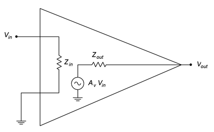
This is a model of a voltage amplifier (note that Vin and Vout are specified along with a controlled voltage source within the model). The controlled voltage source and its series Zout is the Thevenin equivalent of the output when viewed from the load (i.e., the Vout pin). Likewise, Zin is the equivalent impedance seen by the driving source. Because a voltage amplifier is designed to maximize voltage transfer, the input impedance tends to be high to minimize loading (think of a voltmeter). Similarly, the output impedance would tend to be low (think of an ideal voltage source). In contrast, a circuit designed for maximum current transfer would tend to have a low Zin and a high Zout. Precisely how the circuit creates the signal boost is not a concern of this model, we only care that it does.
Loading Effects
Once the model is established it is relatively easy to recognize and compute loading effects. Loading effects are signal losses caused by interactions between the amplifier’s impedances and those of the circuits and loads connected to it. A generic model including loading effects is shown in Figure 5.2.2.
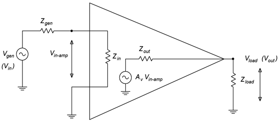
A cursory examination of Figure 5.2.2 shows that there is a voltage divider between Zgen and Zin along with a second divider between Zout and Zload. Each of these dividers causes signal loss, that is, they reduce the final output voltage. The input voltage to the amplifier is reduced as follows:
![\[ V_i_n _- _a_m_p = \frac {Z_i_n}{Z_i_n + Z_g_e_n } \times V_g_e_n \]](https://pressbooks.nscc.ca/app/uploads/quicklatex/quicklatex.com-6682ba5c589dab0ac65f4d78b4cfbf4a_l3.png "Rendered by QuickLaTeX.com")
The load voltage is reduced as follows:
![\[ V_i_n _- _a_m_p = \frac {Z_l_o_a_d}{Z_l_o_a_d + Z_o_u_t } x A_v \times V_i_n - amp \]](https://pressbooks.nscc.ca/app/uploads/quicklatex/quicklatex.com-2caf7234585d8ee63fa18f4c9c642562_l3.png "Rendered by QuickLaTeX.com")
Therefore the combined gain is:
![\[ A _s_y_s_t_e_m = \frac {V _l_o_a_d}{V _g_e_n} = \frac {Z _i_n}{Z _i_n+ Z _g_e_n} \times A_v \times \frac {Z _l_o_a_d}{Z _l_o_a_d + Z _o_u_t} \]](https://pressbooks.nscc.ca/app/uploads/quicklatex/quicklatex.com-986af4a17de1953721b017d959e6ff43_l3.png "Rendered by QuickLaTeX.com")
To minimize these losses we’d like Zin ≫ Zgen and Zload ≫ Zout .
A voltage amplifier has the following specifications: Av = 20 , Zin = 10 kΩ, Zout = 200Ω. It is driven by a 30 millivolt source with a 600 Ω internal impedance and drives a 1 kΩ load. Determine the load voltage.
The voltage that appears at the amplifier’s input is
![\[ V_i_n _- _a_m_p = \frac {Z_i_n}{Z_i_n + Z _g_e_n} \times V _g_e_n \]](https://pressbooks.nscc.ca/app/uploads/quicklatex/quicklatex.com-6eb24024ee917f7c2b7743cee5398e6b_l3.png "Rendered by QuickLaTeX.com")
![\[ V_i_n _- _a_m_p = \frac {10 k \Omega}{10 k \Omega + 600 \Omega} \times 30mV \]](https://pressbooks.nscc.ca/app/uploads/quicklatex/quicklatex.com-6a4056d7260debe65b3920d3762f0036_l3.png "Rendered by QuickLaTeX.com")
![\[ V_i_n _- _a_m_p = 28.3mV \]](https://pressbooks.nscc.ca/app/uploads/quicklatex/quicklatex.com-c8e1978dea487c5794cd617e95c9d112_l3.png "Rendered by QuickLaTeX.com")
This is multiplied by the voltage gain of 20 and then reduced by the output divider.
![\[ V_i_n _- _a_m_p = \frac{Z_l_o_a_d}{Z_l_o_a_d = Z_o_u_t} \times A_v \times V_i_n_-_a_m_p \]](https://pressbooks.nscc.ca/app/uploads/quicklatex/quicklatex.com-c8f49be3c4cbb17246925f259a1c7be2_l3.png "Rendered by QuickLaTeX.com")
![\[ V_i_n _- _a_m_p = \frac {1 k \Omega}{1 k \Omega + 200 \Omega} \times 20 \times 28.3mV \]](https://pressbooks.nscc.ca/app/uploads/quicklatex/quicklatex.com-41b1a5e6fd2d3ad80d65c8bb72665fed_l3.png "Rendered by QuickLaTeX.com")
![\[ V_i_n _- _a_m_p =471.7mV \]](https://pressbooks.nscc.ca/app/uploads/quicklatex/quicklatex.com-5cc6491e9aa63e4487f56ce27dc04141_l3.png "Rendered by QuickLaTeX.com")
Without the loading effects the output signal would be simply 30 millivolts times the voltage gain of 20, or 600 millivolts. Further, note that if the source is replaced with a typical laboratory grade function generator exhibiting an internal impedance of 50 Ω and the load is removed, being replaced by an oscilloscope exhibiting a typical 1 MΩ input impedance, the loading effects would be minimal and we would measure just a few millivolts shy of the ideal 600 millivolts.
