
7.3 Class A Operation and Load Lines
The signal current in the class A amplifier flows continuously throughout the entire cycle of the waveform. Ultimately, we would like to known just how large this signal can be before it is limited and grossly distorted. To do so, we need to examine the AC equivalent of the amplifier. A generic AC equivalent is shown in Figure 7.3.1. This includes both AC collector and emitter resistances so it can be used for either swamped or unswamped common emitter amplifiers or for emitter followers. If one of the resistances is not used (for example, rC in a follower), we can just substitute a value of zero for it.
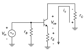
The voltage polarities and current direction are shown for a positive input voltage. To determine the maximum load voltage swing (compliance), we will need to construct an AC load line as shown in Figure 7.3.2.
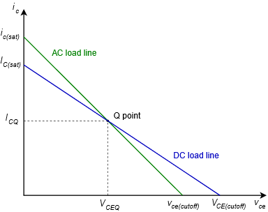
The AC load line is similar to the DC load line that was used for analyzing biasing circuits. As in the DC version, there will be a cutoff voltage, VCE(cutoff), and a saturation current, IC(sat) . The AC and DC load lines normally are not the same, however, they must share one point in common, and that’s the Q point. Usually, the slope of the AC load line is steeper than that of the DC load line. This is because the AC resistance tends to be less than the DC resistance due to loading and capacitor bypassing. Consequently, VCE(cutoff) tends to be smaller than VCE(cutoff) and IC(sat) tends to be larger than IC(sat).
ICQ and a no-signal transistor voltage of VCEQ. As the input signal grows, iC increases. The effect of this is to increase the voltage drops across rE and rC due to Ohm’s law. This, in turn, forces VCE to decrease due to KVL. The collector current can only increase to the point where VCE drops to 0 V. This is a maximum increase of VCEQ/(rC + rE ) . Therefore
![\[I_{C(sat )} = I_{CQ} + \frac{V_{CEQ}}{r_E+r_C} \]](https://pressbooks.nscc.ca/app/uploads/quicklatex/quicklatex.com-3215c08590510fbf02a62aee9b1d8cdb_l3.png "Rendered by QuickLaTeX.com") (7.3.1)
(7.3.1)
In terms of cutoff voltage, the transistor starts with VCEQ and ICQ. The largest vCE increase that can occur is if the current falls to zero. Then, all of the potential originally developed across rE and rC by ICQ must be absorbed by the transistor. Therefore
![\[V_{CE (cutoff )} = V_{CEQ} +I_{CQ} (r_E+r_C ) \]](https://pressbooks.nscc.ca/app/uploads/quicklatex/quicklatex.com-6ef444e722871b4b2a25e03e35c09fe3_l3.png "Rendered by QuickLaTeX.com")
(7.3.2)
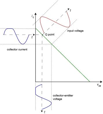
There are three possible ways this can be configured: Q point closer to saturation, Q point closer to cutoff, or Q point centered on the AC load line. Let’s first consider the Q point closer to saturation. This is shown in Figure 7.3.3.
Here we have plotted the input voltage in red and drawn the corresponding collector current and collector-emitter voltage in blue. It is apparent that as the input signal increases, eventually, the output signal is limited at zero for VCE and at IC(sat) for IC . The two blue waveforms are severely clipped and distorted. The largest unclipped peak voltage swing is VCEQ and the largest peak current swing is IC(sat) − ICQ , or more conveniently, VCEQ/(rE + rC ) .
If we shift the Q point toward cutoff, we solve the saturation clipping problem but now we have a new problem, as illustrated in Figure 7.3.4. It should come as no surprise that we now have cutoff clipping.
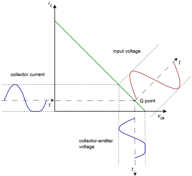
In this version the largest unclipped peak voltage swing is VCE(cutoff) − VCEQ (or alternately, ICQ(rE + rC )) and the largest peak current swing is ICQ. What’s important here is that the waveform has been clipped. It doesn’t really matter which side has been clipped, either way it’s gross distortion. Eventually, every amplifier will have a limit but we will be able to produce the largest unclipped voltage swing if the Q point is centered on the AC load line. This is shown in Figure 7.3.5.
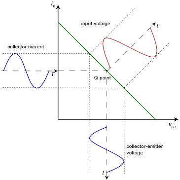
VCEQ and the largest unclipped peak current swing is ICQ. By examining equations 7.3.1 and 7.3.2 it is apparent that in order to achieve a centered Q point on the AC load line, the following must be true:
![\[\frac{V_{CEQ}}{I_{CQ}} = r_E+r_C \]](https://pressbooks.nscc.ca/app/uploads/quicklatex/quicklatex.com-c559b3e79987d7e0e6ef8c77f1ef046e_l3.png "Rendered by QuickLaTeX.com")
(7.3.3)
Of course, while it is useful to determine the maximum voltage across the transistor, it is more important to determine the maximum voltage across the load. Looking back at the circuit of Figure 7.3.1, most times the maximum load voltage (i.e., the compliance) will equal the maximum transistor voltage. This will be the case in voltage followers and unswamped amplifiers. The only time there will be a noticeable reduction is with very heavily swamped amplifiers. In this case the compliance will be reduced by the voltage divider between the load and swamping resistors. For example, a swamped amplifier with a voltage gain of 4 would lose about 20% of the maximum swing. Swamping has to be very heavy resulting in very low gains before appreciable signal is lost.
Thus we arrive at the following general rule:
![\[\text{Peak compliance is the smaller of } V_{CEQ} \text{ or } I_{CQ}(r_E+r_C) \]](https://pressbooks.nscc.ca/app/uploads/quicklatex/quicklatex.com-979bee71450d0bc93c2ce1a16a0d5756_l3.png "Rendered by QuickLaTeX.com")
Knowing the compliance, the maximum load power may be determined using power law. Power is determined using RMS values, so the peak compliance will need to be divided by √2 (or multiplied by 0.707) before continuing.
![\[P_{load (max)} = \frac{{Compliance_{RMS}}^2}{R_L} \]](https://pressbooks.nscc.ca/app/uploads/quicklatex/quicklatex.com-3f14fb4ff2ca20f4473f1bed46e57236_l3.png "Rendered by QuickLaTeX.com")
(7.3.5)
There is something important to note about this equation. It uses the load resistance value, not the total AC effective value (i.e., not rL which is RL in parallel with a biasing resistor). If rL was used, we’d be calculating the power in the load plus the power in the biasing resistor.
We would also like to determine the maximum power dissipated by the transistor. Because the transistor’s current and voltage are fluctuating with the input signal, we need to determine the magnitude of the load voltage that produces maximum power in the transistor. Intuitively, we might guess that this occurs at maximum load power but it turns out that this guess is incorrect. Under no- signal conditions the transistor is operating statically at the Q point. Therefore, quiescent power dissipation is
![\[P_{DQ} = V_{CEQ} I_{CQ} \]](https://pressbooks.nscc.ca/app/uploads/quicklatex/quicklatex.com-5a9f4ecf45dfc02f3bc8614f38b295ec_l3.png "Rendered by QuickLaTeX.com")
(7.3.6)
In contrast, at full load for a centered Q point, we have
![\[V_{CE} = V_{CEQ} (1-\sin 2 \pi ft) \]](https://pressbooks.nscc.ca/app/uploads/quicklatex/quicklatex.com-1fd9fe7b4e3a6e9dff2e1e4b45413eae_l3.png "Rendered by QuickLaTeX.com")
![\[I_C = I_{CQ} (1+ \sin 2 \pi ft) \]](https://pressbooks.nscc.ca/app/uploads/quicklatex/quicklatex.com-d43d1f15f976f927c2535e7bc795ee8f_l3.png "Rendered by QuickLaTeX.com")
![\[P_D = v_{CE} i_C \]](https://pressbooks.nscc.ca/app/uploads/quicklatex/quicklatex.com-ca13e05443c434baac0cdeb7ba71049c_l3.png "Rendered by QuickLaTeX.com")
![\[P_D = V_{CEQ} (1− \sin 2 \pi ft) \times I_{CQ} (1+ \sin 2 \pi ft)\]](https://pressbooks.nscc.ca/app/uploads/quicklatex/quicklatex.com-d4baefe1ec4341267c7115719bd366ca_l3.png "Rendered by QuickLaTeX.com")
![\[P_D = V_{CEQ} I_{CQ} (1-\sin^2 2 \pi ft) \]](https://pressbooks.nscc.ca/app/uploads/quicklatex/quicklatex.com-892c4a0f5e6047ad3eaa8ccfa69d2d9b_l3.png "Rendered by QuickLaTeX.com")
![\[P_D = V_{CEQ} I_{CQ} (.5+.5 \cos 4 \pi ft) \]](https://pressbooks.nscc.ca/app/uploads/quicklatex/quicklatex.com-0a1d8fdb7cbc6e596eee74cdc386bd47_l3.png "Rendered by QuickLaTeX.com")
![\[P_D = \frac{P_{DQ}}{2} + \frac{P_{DQ}}{2} \cos 4 \pi ft \]](https://pressbooks.nscc.ca/app/uploads/quicklatex/quicklatex.com-5adaf431ec77074106a6b571671e3614_l3.png "Rendered by QuickLaTeX.com")
(7.3.7)
The first term of Equation 7.3.7 is a fixed offset while the second term is a sinusoid at twice the signal frequency. Because the peak amplitude of this sinusoid is the same as the fixed offset, the average over time is simply the offset value. These waveforms are illustrated in Figure 7.3.6.
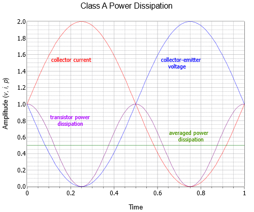
ICQ. That current times the supply voltage yields the supplied power. What’s happening is that as the signal increases in amplitude, more and more of the power dissipated by the transistor is shifted to the load. At maximum load swing, both the transistor and the load will be dissipating PDQ/2. As strange as it might seem, if you want to keep the output transistor of a class A amplifier cool, don’t turn the volume down, turn it up.
The foregoing implies that class A designs are not power efficient. This is indeed the situation. As we have just seen, the best case maximum load power will be one half of PDQ, assuming a centered Q point (non-centered will be worse). To achieve this swing, the power supply will have to be at least twice as large as VCEQ because it has to cover the peak-to-peak swing, while VCEQ represents the peak swing for a centered Q point.[1] In any event, the best case efficiency turns out to be dismal, as follows.
![\[\eta = \frac{P_{out}}{P_{i n}} = \frac{P_{load}}{P_{DC}} \]](https://pressbooks.nscc.ca/app/uploads/quicklatex/quicklatex.com-a291aedd08a2fbcbcdbffa310e3bbe8f_l3.png "Rendered by QuickLaTeX.com")
![\[\eta = \frac{P_{DQ} /2}{2V_{CEQ} I_{CQ}} \]](https://pressbooks.nscc.ca/app/uploads/quicklatex/quicklatex.com-b0c29e49fb5e0d7233596c66a25b5fc9_l3.png "Rendered by QuickLaTeX.com")
![\[\eta = \frac{P_{DQ} / 2}{2 P_{DQ}} \]](https://pressbooks.nscc.ca/app/uploads/quicklatex/quicklatex.com-72122a3000494452f16e190b015016f0_l3.png "Rendered by QuickLaTeX.com")
![\[\eta = 25 \% \]](https://pressbooks.nscc.ca/app/uploads/quicklatex/quicklatex.com-c6d420c2d45eda4fbb55f28fafa62155_l3.png "Rendered by QuickLaTeX.com")
This represents the maximum or best case efficiency for an RC coupled class A amplifier. It may be considerably less depending on precisely how it is biased. This, truly, is the Achilles heel of the class A topology: it is wasteful. It draws full power from the supply regardless if signal is present and, at best, will translate only one quarter of that power into useful load power. At the same time, the power dissipation of the transistor will need to be at least twice that of the delivered load power, and might need to be much greater. Why use it then? To its advantage, it is a relatively simple design so if large output powers are not needed, it can
Example 7.3.1
For the amplifier shown in Figure 7.3.7, determine the compliance, maximum load power, worst case transistor dissipation and efficiency.
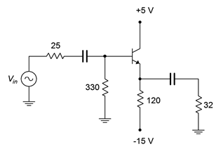
![\[I_{CQ} = \frac{|V_{EE}|-V_{BE}}{R_E} \]](https://pressbooks.nscc.ca/app/uploads/quicklatex/quicklatex.com-a56e9c801b37f6a8f9324e55a2562fe1_l3.png "Rendered by QuickLaTeX.com")
![\[I_{CQ} = \frac{15 V-0.7 V}{120 \Omega} \]](https://pressbooks.nscc.ca/app/uploads/quicklatex/quicklatex.com-eb27fcb1fed6edd82b62f198176b5d1e_l3.png "Rendered by QuickLaTeX.com")
![\[I_{CQ} = 119mA \]](https://pressbooks.nscc.ca/app/uploads/quicklatex/quicklatex.com-82c868e24003c17699fc58fa73747d52_l3.png "Rendered by QuickLaTeX.com")
By inspection, VCEQ = 5.7 V. The AC cutoff voltage is
![\[V_{CE (cutoff )} = V_{CEQ} +I_{CQ} (r_C+r_E ) \]](https://pressbooks.nscc.ca/app/uploads/quicklatex/quicklatex.com-9c651ce9c8e196ab6f76331e3da4032d_l3.png "Rendered by QuickLaTeX.com")
![\[V_{CE (cutoff )} = 5.7 V+119mA(0+120 \Omega || 32 \Omega ) \]](https://pressbooks.nscc.ca/app/uploads/quicklatex/quicklatex.com-d9e7639eceee50f277bb7af467f0aa16_l3.png "Rendered by QuickLaTeX.com")
![\[V_{CE (cutoff )} = 5.7 V+119mA(25.3 \Omega ) \]](https://pressbooks.nscc.ca/app/uploads/quicklatex/quicklatex.com-0ae02afcd07e9e4e70a6594e1a3dbd74_l3.png "Rendered by QuickLaTeX.com")
![\[V_{CE (cutoff )} = 5.7 V+3V \]](https://pressbooks.nscc.ca/app/uploads/quicklatex/quicklatex.com-cfc28ae4d2eb8be90ba9d8cc2d9264ac_l3.png "Rendered by QuickLaTeX.com")
![\[V_{CE (cutoff )} = 8.7 V \]](https://pressbooks.nscc.ca/app/uploads/quicklatex/quicklatex.com-f57401c1e36d2b3137016b6d1da0a34c_l3.png "Rendered by QuickLaTeX.com")
The smaller of VCEQ and ICQ(rC + rE ) is the peak compliance, so
![\[compliance = 3 V peak \]](https://pressbooks.nscc.ca/app/uploads/quicklatex/quicklatex.com-79977000669ed609863ad4d3bd318465_l3.png "Rendered by QuickLaTeX.com")
Given the compliance, we can use power law to find the load power
![\[P_{load (max)} = \frac{(.707 \times 3 V)^2}{32 \Omega} \]](https://pressbooks.nscc.ca/app/uploads/quicklatex/quicklatex.com-646d88aed4c40a9239b815fdfae01b53_l3.png "Rendered by QuickLaTeX.com")
![\[P_{load (max)} = 141mW \]](https://pressbooks.nscc.ca/app/uploads/quicklatex/quicklatex.com-06cf8286311af4e2ca039bac1983fa97_l3.png "Rendered by QuickLaTeX.com")
This is not a lot of power for something like a loudspeaker but is a fair amount to drive something like a pair of headphones.
The transistor’s worst case power dissipation is
![\[P_{D (max)} = P_{DQ} = I_{CQ} V_{CEQ} \]](https://pressbooks.nscc.ca/app/uploads/quicklatex/quicklatex.com-005f87483c14b087e982e7a968f810a4_l3.png "Rendered by QuickLaTeX.com")
![\[P_{D (max)} = 119mA \times 5.7V \]](https://pressbooks.nscc.ca/app/uploads/quicklatex/quicklatex.com-fb201b7829af32dcb42e010fd453138d_l3.png "Rendered by QuickLaTeX.com")
![\[P_{D (max)} = 678mW \]](https://pressbooks.nscc.ca/app/uploads/quicklatex/quicklatex.com-df634d50cf253508d9107cdb557d7250_l3.png "Rendered by QuickLaTeX.com")
The supplied circuit power is the average current draw times the total supplied voltage differential
![\[P_{DC} = I_{CQ} (V_{CC} −V_{EE}) \]](https://pressbooks.nscc.ca/app/uploads/quicklatex/quicklatex.com-2b88269e30c9d8fb124a8b559ce42238_l3.png "Rendered by QuickLaTeX.com")
![\[P_{DC} = 119mA \times 20 V \]](https://pressbooks.nscc.ca/app/uploads/quicklatex/quicklatex.com-64c69e55c84252f97dcd01cefee395a8_l3.png "Rendered by QuickLaTeX.com")
![\[P_{DC} = 2.38W \]](https://pressbooks.nscc.ca/app/uploads/quicklatex/quicklatex.com-159e98ec3e60ea1e38330296d459a9b5_l3.png "Rendered by QuickLaTeX.com")
The efficiency is the ratio of maximum load power to supplied DC power
![\[\eta = \frac{P_{load (max )}}{P_{DC}} \]](https://pressbooks.nscc.ca/app/uploads/quicklatex/quicklatex.com-23d67eb13eaa295c9c083e3c0014fd35_l3.png "Rendered by QuickLaTeX.com")
![\[\eta = \frac{141mW}{2.38 W} \]](https://pressbooks.nscc.ca/app/uploads/quicklatex/quicklatex.com-9f9d42cf0d19876b2d25d9bae142fd7d_l3.png "Rendered by QuickLaTeX.com")
![\[\eta = 5.9 \% \]](https://pressbooks.nscc.ca/app/uploads/quicklatex/quicklatex.com-e785c386b49423b146cd8bae963a88b2_l3.png "Rendered by QuickLaTeX.com")
This is much worse than the theoretical best case. This is due, at least in part, to the fact that the Q point is not centered on the AC load line.
To complete the analysis, note that the transistor’s breakdown rating (BVCEO ) should be at least as large as VCE(cutoff) (8.7 volts), and the maximum current rating should be at least as large as IC(sat) (119 mA+5.7 V/25.3 Ω = 344 mA).
Computer Simulation
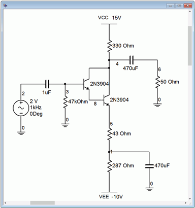
A computer simulation of a class A emitter follower using a Darlington pair is examined next. Of primary interest here is the verification of the output compliance so a transient analysis will be used. The simulator schematic is shown in Figure 7.3.8.
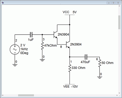
We can make a few quick computations to determine the compliance. First, we find the collector Q point current.
![\[I_{CQ} = \frac{10 V-1.4 V}{330 \Omega} \]](https://pressbooks.nscc.ca/app/uploads/quicklatex/quicklatex.com-08a4f050599c45cf7bcbe41977b9e0a9_l3.png "Rendered by QuickLaTeX.com")
![\[I_{CQ} = 26mA \]](https://pressbooks.nscc.ca/app/uploads/quicklatex/quicklatex.com-a06f0f5df36a6489f271a46e86ab6e67_l3.png "Rendered by QuickLaTeX.com")
By inspection, the emitter is two base-emitter junction potentials below ground, or −1.4 V. As the collectors are tied to VCC , this means that VCEQ = 6.4 V. The other half of the swing, from VCEQ to vCE(cutoff) is
![\[V_{CE (cutoff )}-V_{CEQ} = I_{CQ}(r_C+r_E ) \]](https://pressbooks.nscc.ca/app/uploads/quicklatex/quicklatex.com-619914fe507162bc01e2c8fd1b6cca13_l3.png "Rendered by QuickLaTeX.com")
![\[V_{CE (cutoff )}-V_{CEQ} = 26mA(0+330 \Omega || 50 \Omega ) \]](https://pressbooks.nscc.ca/app/uploads/quicklatex/quicklatex.com-31131e0b1edd46509f4ad10de46880f3_l3.png "Rendered by QuickLaTeX.com")
![\[V_{CE (cutoff )}-V_{CEQ} = 26mA( 43.4 \Omega ) \]](https://pressbooks.nscc.ca/app/uploads/quicklatex/quicklatex.com-77dd8fdaf7122011261683c234f8e06c_l3.png "Rendered by QuickLaTeX.com")
![\[V_{CE (cutoff )}-V_{CEQ} = 1.13V \]](https://pressbooks.nscc.ca/app/uploads/quicklatex/quicklatex.com-7b3fc81dad797816efde0e34a3eb2696_l3.png "Rendered by QuickLaTeX.com")
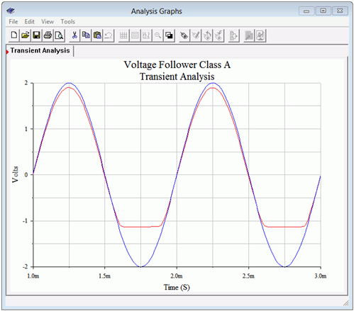
The Q point is not centered and is closer to cutoff. This means that the amplifier will produce cutoff clipping around 1.1 volts and saturation clipping around 6 volts. In other words, there is more room for the current to swing up to saturation than to swing down to zero. As this is the current flowing through the load and we have a non-inverting follower, we expect to see the load voltage echo this. That is, the negative portion of the load voltage should clip before the positive portion.
The transient analysis results are shown in Figure 7.3.9. A two volt peak input signal is applied (blue trace). The negative portion of the load voltage clips at approximately 1.1 volts as expected (red trace). The input signal is not large enough to cause saturation clipping. This was done on purpose to verify the voltage gain of the follower. It should be very close to unity. In fact, the trace shows that the gain is around 0.95 or so.
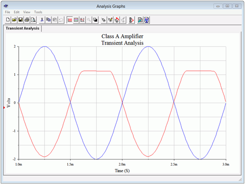
If this had been a voltage amplifier instead of a follower, these waveforms would appear flipped vertically. To verify this, the circuit is modified to produce a voltage amplifier with a gain of approximately one. This is achieved by moving the load to the collector and adding a 330 Ω biasing resistor. This will result in the same AC load impedance. To maintain a similar VCEQ, VCC is raised by 10 volts. Finally, the original 330 Ω emitter biasing resistor is split in two: 287 Ω and 43 Ω. This will yield the same ICQ and achieve a voltage gain of unity. As a result, we expect to see clipping at approximately 1.1 volts on the positive portion. The modified circuit is shown in Figure 7.3.10and the resulting transient simulation in Figure 7.3.11.
One final item of interest regarding the simulations: If the input level is increased in an attempt to see clipping on the other half of the waveform, something strange happens. At first it will appear as though it never clips. A careful examination reveals something different, though. Given the values in these circuits, they will exhibit a certain amount of clamping action (clamping was presented in Chapter 3). This will cause the waveform to shift. If you inspect the peak-to-peak value, it will be close to the value of VCE(cutoff). It will be a little less due to the fact that, particularly for a Darlington pair, VCE(sat) is not 0 V.
- This is the case if the AC and DC load lines are identical. This is atypical. Consequently, the power supply will tend to be larger than twice VCEQ which makes the situation even worse. ↵
