
6.5 Common Base Amplifier
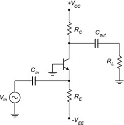
The third and final prototype is the common base amplifier. In this configuration the input signal is applied to the emitter and the output is taken from the collector. The base terminal is at the common ground point. An example, using two-supply emitter bias, is shown in Figure 6.5.1. Note that because neither the input nor output is connected to the base, there is no need for a base resistor. Consequently, the base terminal is connected directly to ground.
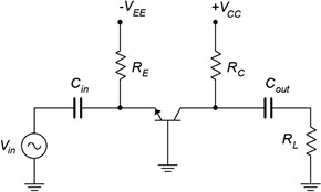
Some people find that redrawing the schematic horizontally helps to visualize the signal flow. This version is shown in Figure 6.5.2.
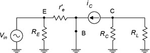
One nice thing about the horizontal version is that when we make the AC equivalent, it becomes obvious that RE is in parallel with the input and RC is in parallel with the load. For the AC analysis we shall modify Figure 6.5.2 by substituting the BJT model for transistor, shorting the capacitors and taking the DC sources to AC ground. The result is shown in Figure 6.5.3.
Voltage Gain
We begin with the basic definition of voltage gain and then expand using Ohm’s law.
![\[A_v = \frac{v_{out}}{v_{i n}} = \frac{v_C}{v_E} \]](https://pressbooks.nscc.ca/app/uploads/quicklatex/quicklatex.com-5105b7c0f61aac59c73e94dbc0ee7283_l3.png "Rendered by QuickLaTeX.com")
![\[A_v = \frac{i_C r_C}{i_E r'_e} \]](https://pressbooks.nscc.ca/app/uploads/quicklatex/quicklatex.com-8370695d4d338576022f31e214dcad4b_l3.png "Rendered by QuickLaTeX.com")
![\[A_v = \frac{r_C}{r'_e} \]](https://pressbooks.nscc.ca/app/uploads/quicklatex/quicklatex.com-0827a95e6c06bb4c74286c29ac4c7b54_l3.png "Rendered by QuickLaTeX.com")
(6.5.1)
This equation is very similar to that of a non-swamped common emitter amplifier except that it does not invert the input signal. Therefore, gain potential is fairly high.
Input Impedance
The derivation for Zin is obtained via direct inspection of the schematic.
![\[Z_{in} = R_E || r'_e \]](https://pressbooks.nscc.ca/app/uploads/quicklatex/quicklatex.com-09bc9ab9e654bfe63a62674b1f8089b2_l3.png "Rendered by QuickLaTeX.com")
(6.5.2)
r’e normally dominates and thus we see that the common base configuration tends to have a low input impedance. For audio frequencies this can be an issue but it is less of a problem at higher frequencies as, generally speaking, system impedances need to be lower to avoid complications with capacitive effects.
Output Impedance
The derivation for Zout unchanged compared to the common emitter configuration. The formula is repeated below for convenience.
![\[Z_{out} \approx R_C \]](https://pressbooks.nscc.ca/app/uploads/quicklatex/quicklatex.com-a4e99589cbc6879eafeb60e3226b219f_l3.png "Rendered by QuickLaTeX.com")
Example 6.5.1
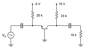
![\[I_C = \frac{∣V_{EE}∣−V_{BE}}{R_E} \]](https://pressbooks.nscc.ca/app/uploads/quicklatex/quicklatex.com-f09c1c84b46adbe9407deabe566fd081_l3.png "Rendered by QuickLaTeX.com")
![\[I_C = \frac{5V-0.7V}{20 k\Omega} \]](https://pressbooks.nscc.ca/app/uploads/quicklatex/quicklatex.com-171439074b130728805c40de3130f5a6_l3.png "Rendered by QuickLaTeX.com")
![\[I_C = 0.215mA \]](https://pressbooks.nscc.ca/app/uploads/quicklatex/quicklatex.com-ae863fef3180838f514fc2c375d5bc32_l3.png "Rendered by QuickLaTeX.com")
![\[r'_e = \frac{26mV}{I_C} \]](https://pressbooks.nscc.ca/app/uploads/quicklatex/quicklatex.com-88217ee3aaf9ce74bd2c97a358034177_l3.png "Rendered by QuickLaTeX.com")
![\[r'_e = \frac{26 mV}{0.215mA} \]](https://pressbooks.nscc.ca/app/uploads/quicklatex/quicklatex.com-36beb050f134ebb6b938eb00fe01058c_l3.png "Rendered by QuickLaTeX.com")
![\[r'_e = 121\Omega \]](https://pressbooks.nscc.ca/app/uploads/quicklatex/quicklatex.com-861034682c28c0c74370a76c9b2ef4bb_l3.png "Rendered by QuickLaTeX.com")
![\[Z_{i n} = 120\Omega \]](https://pressbooks.nscc.ca/app/uploads/quicklatex/quicklatex.com-d7e7b6262792f4e6897f76634b99ce73_l3.png "Rendered by QuickLaTeX.com")
![\[A_v = \frac{33k \Omega || 10 k\Omega}{120\Omega} \]](https://pressbooks.nscc.ca/app/uploads/quicklatex/quicklatex.com-2dbe1a85ab5a1d635090ac115a260f76_l3.png "Rendered by QuickLaTeX.com")
![\[A_v = 64 \]](https://pressbooks.nscc.ca/app/uploads/quicklatex/quicklatex.com-1c52e159f675e0485c8e80c1bb2ff7bc_l3.png "Rendered by QuickLaTeX.com")
