
2.6 Exercises
Assume diodes are silicon unless stated otherwise
Analysis Problems
- For the circuit of Figure 2.6.1, determine the peak output voltage.
Vsec = 12 volts RMS, Rload = 50 Ω, C1 = 1500 μF.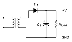
Figure 2.6.1 - Sketch the output voltage waveform for the circuit of Problem 1, Figure 2.6.1, with and without the capacitor.
- Determine the peak output voltage for the circuit of Figure 3.6.2.
Vsec = 18 volts RMS, Rload = 75 Ω, C1 = 470 μF.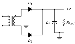
Figure 2.6.2 - Sketch the output voltage waveform for the circuit of Problem 3, Figure 2.6.2, with and without the capacitor.
- For the circuit of Figure 2.6.3, determine the peak output voltage.
Vsec = 18 volts RMS, Rload = 40 Ω, C1 = 1000 μF.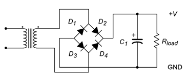
Figure 2.6.3 - Sketch the output voltage waveform for the circuit of Problem 5, Figure 2.6.3, with and without the capacitor.
- Determine the output voltage waveform and its amplitude for the circuit of Figure 3.6.4.
Vin = 10 sin 2π100t, Vclip= 8 volts, R = 10 kΩ.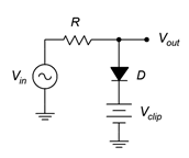
Figure 2.6.4 - Draw the output waveform with its amplitudes for the circuit of Figure 2.6.5.
Vin = 10 sin 2π100t, Vclip = 5 volts, R = 10 kΩ.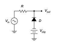
Figure 2.6.5 - Draw the output waveform with its amplitudes for the circuit of Figure 2.6.6.
Vin = 12 sin 2π200t, V1 = 6 volts, V2 = 4 volts, R = 10 kΩ.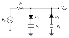
Figure 2.6.6 - Draw the output waveform with its amplitudes for the circuit of Figure 2.6.7.
Vin = 5 sin 2π2000t, C = 10μF, R = 4.7 kΩ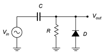
Figure 2.6.7 - Draw the output waveform with its amplitudes for the circuit of Figure 2.6.8.
Vin = 8 sin 2π500t, V clamp = 2 volts, C = 4.7 μF, R = 33 kΩ.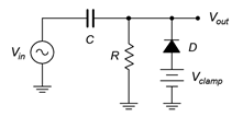
Figure 2.6.8
Design Problems
- Design a 15 volt AC to DC power supply capable of drawing 200 mA.
- Design a circuit that will limit its output voltage to a range of −5 volts to +10 volts.
- Design a circuit that will shift its output voltage so that it is always positive. The input frequency is 2 kHz.
Challenge Problems
- Design a circuit that will shift its output voltage so that its negative peak is at +3 volts. The input frequency range is from 100 Hz to 1 kHz.
Computer Simulation Problems
- Run a transient analysis of the circuit in Figure 2.6.1, Problem 1.
- Run a transient analysis of the circuit in Figure 2.6.2, Problem 3.
- Run a transient analysis of the circuit in Figure 2.6.3, Problem 5.
- Run two transient analyses on the clamper circuit of Example 2.4.1, first using a capacitor 100 times larger than specified, and second using a capacitor 100 times smaller than specified. Discuss the resulting waveforms.
