
7.8 Exercises
Assume diodes are silicon unless stated otherwise
Analysis Problems
- Draw the AC load line for the circuit of Figure 7.8.1. Also determine the compliance, maximum load power, maximum transistor dissipation and efficiency.
VCC = 6 V, VEE = −12 V, Rgen = 50 Ω, RB = 2.2 kΩ, RE = 470 Ω, RL = 75 Ω.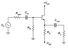
Figure 7.8.1 - Recalculate Problem 1 if the load is halved.
- Determine if the circuit of Figure 7.8.2 has a centered Q point on its AC load line.
VCC = −10 V, VEE = 15 V, RB = 1 kΩ, RE = 330 Ω, RL = 50 Ω.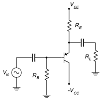
Figure 7.8.2 - Draw the AC load line for the circuit of Figure 7.8.2. Also determine the compliance, maximum load power, maximum transistor dissipation and efficiency.
VCC = −8 V, VEE = 12 V, RB = 1 kΩ, RE = 330 Ω, RL = 32 Ω. - Draw the AC load line for the circuit of Figure 7.8.3. Also determine the compliance, maximum load power, maximum transistor dissipation and efficiency.
VCC = 15 V, VEE = −20 V, RB = 10 kΩ, RE = 100 Ω, RL = 16 Ω.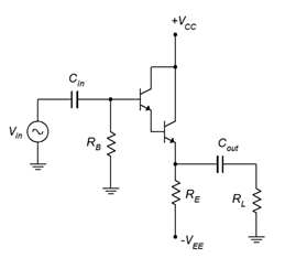
Figure 7.8.3 - Determine if the circuit of Figure 7.8.4 has a centered Q point on its AC load line.
VCC = 30 V, R1 = 3.9 kΩ, R2 = 3.3 kΩ, RE = 560 Ω, RL = 50 Ω.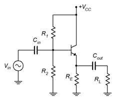
Figure 7.8.4 - Draw the AC load line for the circuit of Figure 7.8.4. Also determine the compliance, maximum load power, maximum transistor dissipation and efficiency.
VCC = 30 V, R1 = 2.2 kΩ, R2 = 2.2 kΩ, RE = 470 Ω, RL = 32 Ω. - Determine if the circuit of Figure 7.8.5 has a centered Q point on its AC load line.
VCC = 15 V, VEE = −15 V, RB = 1 kΩ, RE = 510 Ω, RSW = 10 Ω, RC = 270 Ω, RL = 50 Ω.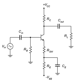
Figure 7.8.5 - Draw the AC load line for the circuit of Figure 7.8.5. Also determine the compliance, maximum load power, maximum transistor dissipation and efficiency.
VCC = 25 V, VEE = −15 V, RB = 1 kΩ, RE = 270 Ω, RSW = 6.8 Ω, RC = 330 Ω, RL = 16 Ω. - A power transistor has a PD(max) of 50 watts at 25°C. It has a derating factor of 0.4 W/C°. Will this transistor be sufficient for a circuit that needs to dissipate 40 watts at 85°C?
- A power transistor has a PD(max) of 100 watts at 25°C. It has a derating factor of 0.6 W/C°. Will this transistor be sufficient for a circuit that needs to dissipate 65 watts at 75°C?
- Determine the appropriate heat sink rating for a power device rated as follows:
Tj(max) = 175°C, TO-3 case style, θjc = 1.5 C°/W. The device will be dissipating a maximum of 25 W in an ambient temperature of 35°C. Assume that the heat sink will be mounted with heat sink grease and a 0.003 mica insulator. - Determine the appropriate heat sink rating for a power device rated as follows:
Tj(max) = 165°C, TO-220 case style, θjc = 3 C°/W. The device will be dissipating a maximum of 15 W in an ambient temperature of 35°C. Assume that the heat sink will be mounted with heat sink grease and a 0.002 mica insulator.
Design Problems
- Alter the emitter power supply in the circuit described in Problem 1 to achieve a centered Q point.
- Alter the emitter power supply in the circuit described in Problem 4 to achieve a centered Q point.
Challenge Problems
- Find a heat sink (make and model number) that will meet the thermal resistance requirement for Problem 12 with no more than 400 feet/minute of forced air.
- Alter the voltage divider in the circuit described in Problem 6 to achieve a centered Q point.
Computer Simulation Problems
- Perform a transient analysis for the circuit described in Problem 1 to verify the compliance.
- Perform a transient analysis for the circuit described in Problem 4 to verify the compliance.
- Perform a transient analysis for the circuit described in Problem 9 to verify the compliance.
