
8.5 Exercises
Analysis Problems
- For the circuit of Figure 8.5.1, determine compliance, Pload(max), PD(max), BVCEO and IC(max).
VCC = 15 V, VEE = −15 V, ß = 75, RL = 16 Ω, R1 = 680 Ω, R2 = 680 Ω. - For the circuit of Figure 8.5.1, determine Zin.
VCC = 15 V, VEE = −15 V, ß = 75, RL = 16 Ω, R1 = 680 Ω, R2 = 680 Ω. - For the circuit of Figure 8.5.1, determine Zin.
VCC = 25 V, VEE = −25 V, ß = 70, RL = 8 Ω, R1 = 560 Ω, R2 = 560 Ω.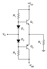
Figure 8.5.1 - For the circuit of Figure 8.5.1, determine compliance Pload(max), and PD(max), BVCEO and IC(max).
VCC = 25 V, VEE = −25 V, ß = 70, RL = 8 Ω, R1 = 560 Ω, R2 = 560 Ω. - For the circuit of Figure 8.5.2, determine Pload(max), and PD(max), BVCEO and IC(max).
VCC = 15 V, ß = 75, RL = 16 Ω, R1 = 630 Ω, R2 = 630 Ω.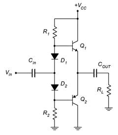
Figure 8.5.2 - For the circuit of Figure 8.5.2, determine Zin.
VCC = 15 V, ß = 75, RL = 16 Ω, R1 = 630 Ω, R2 = 630 Ω. - For the circuit of Figure 8.5.2, determine Zin.
VCC = 25 V, ß = 70, RL = 8 Ω, R1 = 560 Ω, R2 = 560 Ω. - For the circuit of Figure 8.5.2, determine Pload(max), and PD(max), BVCEO and IC(max).
VCC = 25 V, ß = 70, RL = 8 Ω, R1 = 510 Ω, R2 = 510 Ω. - For the circuit of Figure 8.5.3, determine Pload(max), and PD(max), BVCEO and IC(max) for the output transistors.
VCC = 24 V, VEE = −24 V, ß = 75, RL = 8 Ω, R1 = 2.5 kΩ, R2 = 300 Ω, R3 = 330 Ω, R4 = 63 Ω.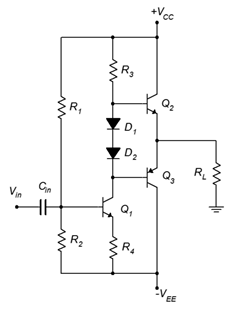
Figure 8.5.3 - For the circuit of Figure 8.5.3, determine Av and Zin.
VCC = 24 V, VEE = −24 V, ß = 75, RL = 8 Ω, R1 = 2.5 kΩ, R2 = 300 Ω, R3 = 330 Ω, R4 = 63 Ω.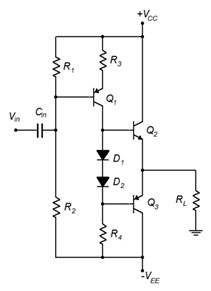
Figure 8.5.4 - For the circuit of Figure 8.5.4, determine Pload(max), and PD(max), BVCEO and IC(max) for the output transistors.
VCC = 24 V, VEE = −24 V, ß = 75, RL = 16 Ω, R1 = 600 Ω, R2 = 5 kΩ, R3 = 63 Ω, R4 = 330 Ω. - For the circuit of Figure 8.5.4, determine Av and Zin.
VCC = 24 V, VEE = −24 V, ß = 75, RL = 16 Ω, R1 = 600 Ω, R2 = 5 kΩ, R3 = 63 Ω, R4 = 330 Ω. - Determine the limit current for the circuit of Figure 8.5.5 if RE = 0.2 Ω.
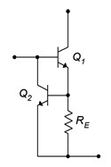
Figure 8.5.5 - Determine Pload(max), and PD(max), BVCEO and IC(max) for the output and driver transistors of Figure 8.5.6.
VCC = 50 V, VEE = −50 V, ß = 75, RL = 8 Ω, R5 through R8 = 0.05 Ω. Assume all other components produce proper bias.
Design Problems
- For the circuit of Figure 8.5.3, determine values for R1 and R2 for proper bias.
VCC = 32 V, VEE = −32 V, ß = 75, RL = 8 Ω, R3 = 330 Ω, R4 = 63 Ω. - Determine a value for RE to set the limit current for the circuit of Figure 8.5.5 to 2 A.
Challenge Problems
- For the circuit of Figure 8.5.6, determine values for R1 and R2 for proper bias.
VCC = 50 V, VEE = −50 V, ß = 85, RL = 8 Ω, R5 through R8 = 0.05 Ω, R3 = 2.2 kΩ, R4 = 330 Ω. - For the circuit of Figure 8.5.7, determine a value for R5 for proper bias.
VCC = 30 V, VEE = −30 V, ß = 100, RL = 16 Ω, R1 = 2.2 kΩ, R2 = 8.2 kΩ, R3 = 1.2 kΩ, R4 = 47 Ω, R5 = 330 Ω, R6 = 470 Ω, R7 = 68 Ω.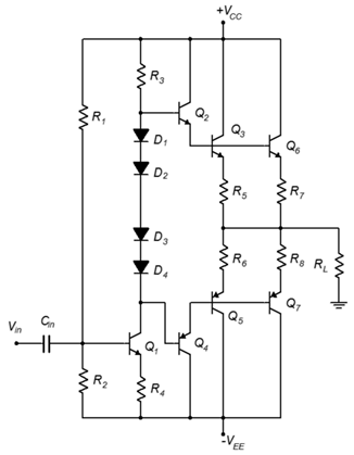
Figure 8.5.6
Computer Simulation Problems
- Perform a transient analysis on the circuit of Problem 1 to verify the compliance.
- Perform a transient analysis on the circuit of Problem 4 to verify the compliance.
- Perform a DC analysis on the design from Problem 15 to verify the results.
- Perform a DC analysis on the design from Problem 17 to verify the results.
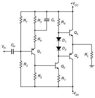
Figure 8.5.7
