
8.3 Extensions and Refinements
The foregoing discussion has covered the basics of class B amplifier design and operation but there are a variety of things we might add.
Current Limiting
One of the more useful additions to an amplifier is some form of protection circuit. As noted earlier, there is nothing in the basic class B amplifier to limit current, so if the load is accidentally shorted, the transistor current will spike to very high levels and possibly damage the output transistors. How might we prevent this from happening?
Perhaps the most basic protection technique is to place a fuse in-line with the load. This is a somewhat tricky proposition because voice and music waveforms are very dynamic. Fuses are not fast response devices and selection of the proper current rating is a trade-off. If we want to catch large, fast transients, the fuse will have to be rated on the low side. Unfortunately, the fuse might then blow on moderately loud sustained low frequency content. Relays suffer from similar problems. Also, there is the issue that if the fuses are replaceable by the consumer, they may use the wrong value or some other item[1] that will allow too much current, resulting in blown output transistors. This can be avoided by having a second set of fuses mounted on the PC board, connected to the power rails, but this is also an imperfect solution.
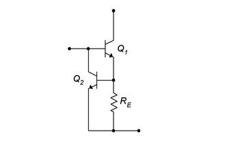
One means of dealing with this situation is to employ an active current limiter, such as the circuit shown in Figure 8.3.1. In this circuit, Q1 is the main NPN output transistor, the PNP side not shown. At the top is the power supply connection and the load is connected off to the right. A small resistor, RE, is inserted into the emitter current path. The resistance is small enough that the voltage across it is normally less than 0.5 volts or so. Across the resistor is another transistor, Q2. Under normal operation Q2 is not on and does not affect the circuit. If the load current gets large enough (beyond the safe limit), the voltage drop across RE will reach 0.7 V. At this point Q2 turns on and begins to conduct current away from the base of Q1, limiting the amount of load current to approximately 0.7V /RE. Unlike a fuse, once the fault is removed and the load current falls to safe levels, Q2 disengages and normal amplifier function resumes.
Two of these circuits are required for the amplifier; one for the positive half and one for the negative half. Figure 8.3.2 shows a class B amplifier with the added current protection circuits (within the dashed red box).
High Current Gain Configurations
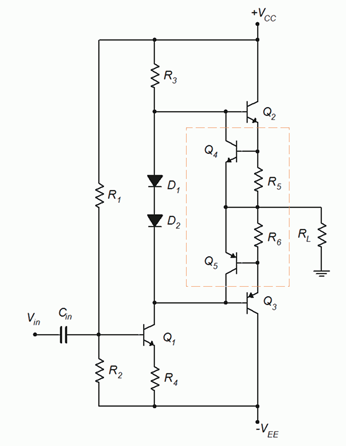
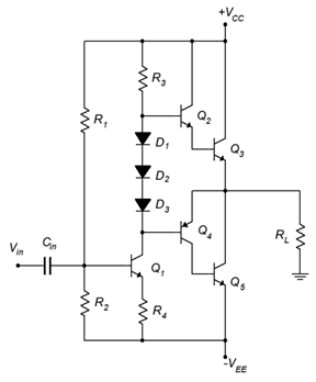
For some applications the β of typical power transistors may prove to be insufficient. In such cases we can use high current gain configurations. There are several ways to configure the output devices. A Darlington scheme is shown in Figure 8.3.3. Q3 and Q5 are the main output devices. Q2 and Q4 can be thought of as drive transistors. Although their BVCEO rating will need to be as high as that of Q3/Q5, they will be handling less current and therefore will dissipate less power. Sometimes Q2/Q4 are configured as seen here and sometimes emitter resistors may be added so that the output appears to be a cascade of emitter followers. Either way, there are now four base-emitter junctions to be compensated for, thus the addition of D3 and D4.
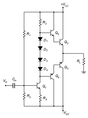
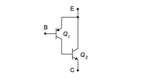
Some years ago, high power PNP transistors exhibiting decent audio quality were not available. Instead of using a PNP Darlington configuration, a Sziklai pair was used. This dual transistor configuration is named after Hungarian, and later, American, engineer George Sziklai. The Sziklai pair is also known as a composite pair. A composite PNP is shown in Figure 8.3.4. The operation is similar to that of a Darlington pair. The input transistor, Q1, drives its collector current into the base of Q2, the output transistor.
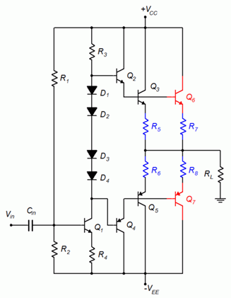
Q2‘s base current is multiplied by its β, thus its collector current is the product of IB1 , β1 and β2, just like a Darlington. The differences are that the main power device for the composite PNP is an NPN, and that there is only a single VBE to compensate for. An example amplifier based on the earlier direct coupled driver circuit is shown in Figure 8.3.5. This configuration is known as a quasi-complementary output.[2] Note the use of three compensating diodes; two for the Darlington NPN and one for the composite PNP/Sziklai pair. One advantage here is that the power devices, Q3 and Q5, can be identical models.
The current limiting circuit of Figure 8.3.1 can be added to both the Darlington and quasi-complementary output stages. Current limiting can also be added to the circuits presented in the next section, but have been left off for clarity.
Current Sharing
For higher output powers, and especially for amplifiers driving very low load impedances such 1 or 2 ohms, it may not be possible to use a single NPN and PNP for the output stage. Instead, the duties of each device will be shared among two or three transistors operating in parallel. Generally, current-sharing schemes will also require a Darlington-based approach due to the very high total load current.
Initially, it may be tempting to just place two or three transistors in parallel, each base terminal being fed by a common drive transistor. There is a fatal flaw with this approach. The issue is referred to as either thermal runaway or current hogging. The basic e problem is that the temperature coefficient of transconductance for a bipolar transistor is positive. In other words, r′ gets smaller as temperature rises. This means that, as the device heats up, it tends to more easily conduct current. Of course, if the device draws more current, it will dissipate more power, which means that it will get hotter, which means that it will conduct more current, which means that it will dissipate more power, and so on. This process spirals out of control and is particularly evil when we have multiple devices in parallel. Devices are never perfectly matched so the load current will never be perfectly shared among the devices. This means that one device will tend to get hotter than the other(s) which leads to it getting even hotter and grabbing a larger and larger share of the total current. Eventually, this device “hogs” all of the available current and winds up destroying itself. What we have is a positive thermal feedback loop. Transistor harakiri is a decidedly sub-optimal performance characteristic. To circumvent this problem we can add small resistors to the emitters of the devices. As all of the paralleled devices are being driven from a common drive transistor, they all see the same base voltage. If one output transistor starts to grab a larger share of the load current, the voltage drop across the emitter resistor will increase, thus forcing a reduction in that transistor’s base-emitter voltage. This reduction compensates for the initial tendency of the current to increase. This technique is referred to as local negative feedback. We have seen this concept before, for example, a swamping resistor falls into this category as does the collector feedback bias scheme.
An example of a current-sharing output section is shown in Figure 8.3.6. This version uses a Darlington scheme. The newly added transistors are shown in red while the thermal/current feedback resistors are shown in blue.
VBE Multiplier and Miller Capacitor
With the ever increasing complexity of the output section, the simple diode biasing scheme lacks the ability to set the optimal idle bias to achieve minimum crossover distortion. A more flexible approach is to use a VBE multiplier, as illustrated in Figure 8.3.7.
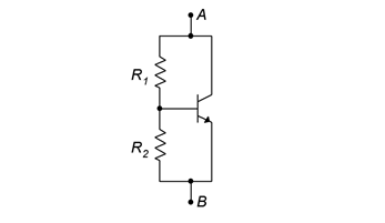
If we ignore base current, the currents through the two resistors are identical. Therefore, their voltages have the same ratio as their resistances. R2 is in parallel with VBE so its voltage must be equal to VBE . Consequently, the voltage across R2 must be a multiple of VBE . For example, if we want to generate the equivalent of four base-emitter drops from point A to point B, we make R1 three times as large as R2 . What makes this particularly useful as that we can set any ratio we want, and by replacing either resistor with a potentiometer, we can make that voltage adjustable. And example is shown in Figure 8.3.8, using the current-sharing amplifier of Figure 8.3.6. The VBE multiplier is shown in the dashed red box and replaces the four biasing diodes. A capacitor, CB, shunts the multiplier, making sure it behaves as a short for AC signals.
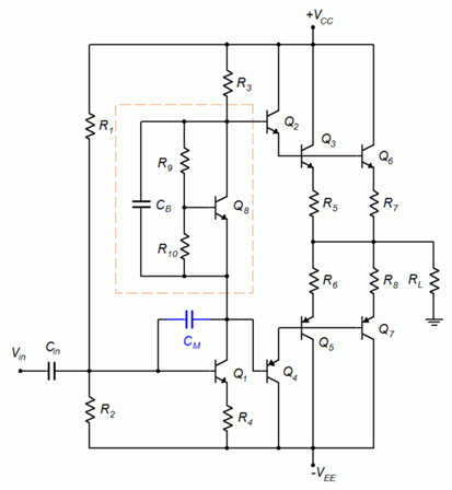
The circuit of Figure 8.3.8 also includes another capacitor, CM . This is a Miller compensation capacitor. It uses the Miller Effect (see Chapter 6, Miller’s Theorem) to create a much larger equivalent input capacitance. This capacitance appears in parallel with the input of Q1 and creates a lag network. The inclusion of CM allows the designer to tailor the high frequency response of the amplifier.
Bridging
Some amplifiers employ a bridged output scheme. This is particularly true where power supply voltages are limited, for example, in automobiles (nominally 12 VDC but closer to 13.8 VDC from the alternator). Without resorting to an expensive DC-to-DC converter, an amplifier designed for automotive use is in a bit of a bind. If we assume a +12 volt DC source, then a basic class B amplifier would use a capacitor coupled configuration like Figure 8.2.6. This would yield a VCEQ of 6 volts and a compliance of about 4.2 volts RMS. If we were to use a standard home loudspeaker of 8 Ω, the maximum load power would be a mere 2.25 watts (this is one reason why car audio systems typically use 4 Ω loudspeakers, because it doubles the output power, in this case to 4.5 watts). A bridged output can double this again.
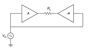
A block diagram of a bridged drive is shown in Figure 8.3.9. The left half is what we would see normally. On the right half we have a second identical amplifier but we drive it with an inverted copy of the original signal. What ends up happening is that, as the left output goes positive, the right output goes negative by the same amount. The end result is that the load sees twice the voltage it would have from the left amplifier alone. Power varies as the square of voltage so doubling the voltage quadruples the power. The 2.25 watt output of that car amplifier jumps up to 9 watts.[3] If we want to go higher than this our only options are to further decrease the loudspeaker impedance (there are practical limits that will not let us go much further) or increase the DC power supply. In the home, increasing the supply is relatively easy as we have an AC power source. In an automotive system this is a much more expensive proposition because only DC is generally available.
An illustration of a bridged system at the transistor level is shown in Figure 8.3.10. For simplicity, this schematic uses basic class B stages. Input and right-side inversion circuitry are not shown.
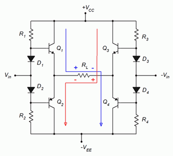
The four transistors create a classic H bridge with the load in the center. For a positive Vin, Q1 turns on. At the same time, because it is being fed by an inverted version of Vin, Q4 turns on. Thus, current flows down from VCC , through Q1 , across RL from left-to-right, down Q4 , and finally to VEE (blue trace). At full swing, the voltage across the load will be VCC − VEE from left to right.
For a negative Vin the opposite happens: Q3 and Q2 turn on, allowing current to flow through RL from right left. The maximum voltage will be the same but with inverted polarity, hence an effective doubling of load voltage and a quadrupling of load power.
This increased output does not come without downsides. The most obvious problem is a doubling of the output circuitry. The second issue may not be immediately apparent: the load is not grounded. In simple automobile audio systems, the chassis of the vehicle is used as the system common or “ground”. Therefore, it is possible to just run a single wire to a loudspeaker from an amplifier’s output. The other loudspeaker terminal is then connected to the chassis at a convenient location. With a bridged output, two wires must be run to the loudspeaker. If a single-lead loudspeaker system is upgraded with a bridged output amplifier, new loudspeaker wires must be installed. Otherwise, the chassis return lead winds up shorting out one side of the bridge.
Power Supply Bypassing
A final comment regarding high power amplifiers, particularly audio amplifiers, is in order. All through this chapter we have assumed that the DC power supplies will act ideally, mainly that they will present themselves as good AC grounds. This is not always easy to achieve given the practical limitations of PC board layouts, wiring constraints and so forth. Consequently, power supply bypass capacitors are often used to ensure a good AC ground. While this was mentioned in Chapter 7 regarding small signal amplifiers, it is perhaps more important for power amplifiers. The power supply bypass capacitors used for power amplifiers tend to be larger and the quality more stringent. A simple 1 μF bypass capacitor would hardly be the norm for a high power audio amplifier. The practical problem is that large, high quality capacitors are not inexpensive. For example, a 10 μF polypropylene capacitor will be at least an order of magnitude more expensive than a similar size aluminum electrolytic (dollars versus cents). Unfortunately, the electrolytic will have higher leakage and ESR, and will not behave nearly as well at high frequencies (indeed, the impedance will actually start to increase due to inductive effects once the frequency gets high enough). To both improve performance and save money, bypass capacitors are sometimes doubled or tripled. For example, a large aluminum electrolytic might be placed in parallel with a much smaller polyester or polypropylene capacitor. The aluminum electrolytic will give the small XC needed at lower frequencies, and when it starts to behave less ideally at higher frequencies, the higher quality poly capacitor effectively shunts it and extends the operating range. The result is nearly as effective as the single large, high quality capacitor but much less expensive.
- Such as bits of wire, aluminum foil, small bolts or screws, etc. Just ask any seasoned repair technician. ↵
- Not to be confused with the quasi-complimentary output of which we have only partially nice things to say. ↵
- OK, not huge, but probably still loud enough to obscure the sirens of emergency vehicles until they're right behind you. ↵
