
7.6 Heat Sinks
The issue with power transistors is always heat. As noted in Example 7.5.1, as the transistor heats up due to internal power dissipation, its ability to dissipate heat is compromised. The trick, then, is to efficiently move the heat from the transistor to someplace else. This is normally achieved through the use of a heat sink.
A heat sink is a metal device that is attached to the power transistor. Typically, they are made of aluminum and feature an array of fins. By increasing the surface area, heat can be moved away from the transistor more efficiently than by the transistor alone.
Heat sinks are designed to mount specific device case styles. The most common case styles include the TO-3 “can” along with the various “power tab” styles such as the TO-220 and TO-202. Special mounting hardware and insulation spacers are also required in order to maintain electrical isolation between the transistor and the heat sink as we do not want the heat sink to be electrically live. This usually takes the form of a mica sheet, and plastic washers and bushings for the mounting machine screws (for small heat sinks, sometimes nylon machine screws are used).
There are a few general rules that should be followed when using heat sinks:
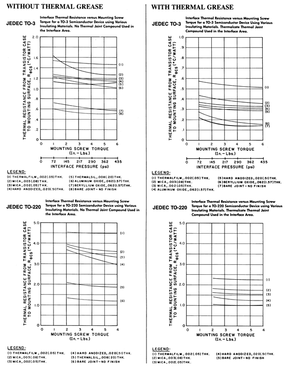
- Always use some form of heat sink grease or thermally conductive pad between the heat sink and the device. This will increase the thermal transfer between the two parts, however, excessive quantities of heat sink grease will decrease performance.
- Mount fins in the vertical plane for optimum natural convective cooling.
- Do not overcrowd or obstruct devices that use heat sinks.
- Do not block air flow around heat sinks – particularly directly above and below items that rely on natural convection.
- If thermal demands are particularly high, consider using forced convection (i.e., a small fan directed at the heat sink).
Some typical heat sinks are shown below. Figure 7.6.1 shows a heat sink and thermal data plot for use with a single TO-3 case device.
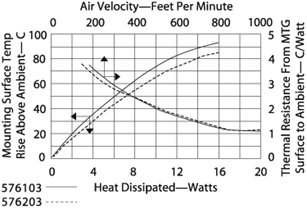
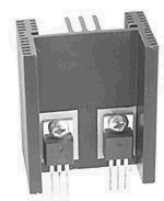
Figure 7.6.2 shows a heat sink designed for a pair of transistors using TO-220 cases. In this photo, the white insulating pads can be seen between the transistors and heat sink.
Thermal Resistance
In order to specify a particular heat sink for a given application, a more technical explanation is in order. What we are going to do is create a thermal circuit equivalent. In this model, the concept of thermal resistance is used. Thermal resistance denotes how easy it is to transfer heat energy from one mechanical part to another. The symbol for thermal resistance is θ, and the units are Celsius degrees per watt. In this model, temperature is analogous to voltage, and thermal power dissipation is analogous to current. A useful equation is,
![\[P_D= \frac{\Delta T}{\theta_{total}} \]](https://pressbooks.nscc.ca/app/uploads/quicklatex/quicklatex.com-7a319f54dfe837a1588de6899042fba3_l3.png "Rendered by QuickLaTeX.com")
(7.6.1)
Where PD is the power dissipated by the semiconductor device in watts, ΔT is the temperature differential, and θtotal is the sum of the thermal resistances. Basically, this is a thermal version of Ohm’s law.
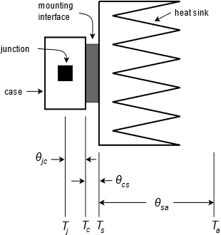
In order to construct our model, let’s take a closer look at the power-device/heat-sink combination. This is shown in Figure 7.6.3. The subscript j stands for junction, c is for case (of the transistor), s is for heat sink and a is for the ambient air. Tj is the semiconductor junction temperature and is created by the product of the transistor’s current and voltage. This thermal source heats the device case to Tc . The thermal resistance between the two entities is θjc . The case, in turn, heats the heat sink via the interconnection. This thermal resistance is θcs , and the resulting temperature is Ts . Finally, the heat sink passes the thermal energy to the surrounding air which is sitting at Ta . The thermal resistance of the heat sink to the air is θsa . The equivalent thermal model is shown in Figure 7.6.4. Although this “thermal circuit” does not have perfect correspondence with normal circuit analysis, it does illustrate the main points.
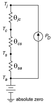
In this model, ground represents a temperature of absolute zero. The circuit is sitting at an ambient temperature Ta , thus a voltage source of Ta is connected to ground and the heat sink. The three thermal resistances are in series and are driven by a current source that is set by the present power dissipation of the device. Note that if the power dissipation is high, the resulting “voltage drops” across the thermal resistances are high. Voltage is analogous to temperature in this model, so this indicates that a high temperature is created. Because there is a maximum limit to Tj, a higher power dissipation requires lower thermal resistances. As θjc is set by the device manufacturer, we have no control over that element. However, θcs is a function of the case style and the insulation material used, so we do have some control (but not a lot) over that. On the other hand, as the person who specifies the heat sink, we have a great deal of control over θsa . Values for θsa are given by heat sink manufacturers. A useful variation of Equation 7.6.1 is
![\[P_D= \frac{T_j-T_a}{\theta_{jc}+\theta_{cs}+\theta_{sa}} \]](https://pressbooks.nscc.ca/app/uploads/quicklatex/quicklatex.com-edc97a16c68ec79dbcb347ea18a527f7_l3.png "Rendered by QuickLaTeX.com")
(7.6.2)
Normally, power dissipation, junction and ambient temperatures, θjc and θcs are known. The idea is to determine an appropriate heat sink. Both Tj and θjc are given by the semiconductor device manufacturer. The ambient temperature, Ta , may be determined experimentally. Due to localized warming, it tends to be higher than the actual “room temperature”. Standard graphs, such as those found in Figure 7.6.5, may be used to determine θcs . Note the generally lower values of θcs for the TO-3 case relative to the TO-220. This is one reason why TO-3 cases are used for higher power devices. This case also makes it easier for the manufacturer to reduce θjc .
Example 7.6.1
![\[P_D= \frac{T_j -T_a}{\theta_{jc}+\theta_{cs}+\theta_{sa}} \]](https://pressbooks.nscc.ca/app/uploads/quicklatex/quicklatex.com-017541ba391a72e79d2b4e8a57858ed5_l3.png "Rendered by QuickLaTeX.com")
![\[\theta_{sa}= T j -Ta P D −\theta jc-\theta cs \]](https://pressbooks.nscc.ca/app/uploads/quicklatex/quicklatex.com-711fbe76855dd48dc7323016cb8e171b_l3.png "Rendered by QuickLaTeX.com")
![\[\theta_{sa}= \frac{175^{\circ}C-40^{\circ}C}{15 W} -1.5C^{\circ}/W-0.35C^{\circ}/W \]](https://pressbooks.nscc.ca/app/uploads/quicklatex/quicklatex.com-34b747dba15864449fa00878b819664c_l3.png "Rendered by QuickLaTeX.com")
![\[\theta_{sa}=7.15C^{\circ}/W \]](https://pressbooks.nscc.ca/app/uploads/quicklatex/quicklatex.com-36acb95dae45e7fc083a8f0c505abbaf_l3.png "Rendered by QuickLaTeX.com")
![\[\theta_{sa}= \frac{T_j -T_a}{P_D} -\theta_{jc}−\theta_{cs} \]](https://pressbooks.nscc.ca/app/uploads/quicklatex/quicklatex.com-eedd8b3f5600a25b5497b2661b3a1eb0_l3.png "Rendered by QuickLaTeX.com")
![\[\theta_{sa}= \frac{175^{\circ}C -40^{\circ}C}{40 W} -1.5C^{\circ}/W -0.35C^{\circ}/W \]](https://pressbooks.nscc.ca/app/uploads/quicklatex/quicklatex.com-720a10fcee53daaad5aff636c0f50717_l3.png "Rendered by QuickLaTeX.com")
![\[\theta_{sa}=1.53C^{\circ}/W \]](https://pressbooks.nscc.ca/app/uploads/quicklatex/quicklatex.com-6b4ae4bbd1d30d65f1c1bc2b7ef1532d_l3.png "Rendered by QuickLaTeX.com")
