
6.2 Simplified AC Model of the BJT
Just as we created a DC model to ease the analysis of DC bias circuits, we shall make use of an AC BJT model for our AC analyses. In fact, our AC model is based on the DC model. The collector-base region is still represented with a current-controlled current source although it’s AC instead of DC: iC = βiB . The base-emitter junction is a bit trickier. Although a simple 0.7 volt junction worked fine for DC, we now have to consider the AC resistance of the diode.
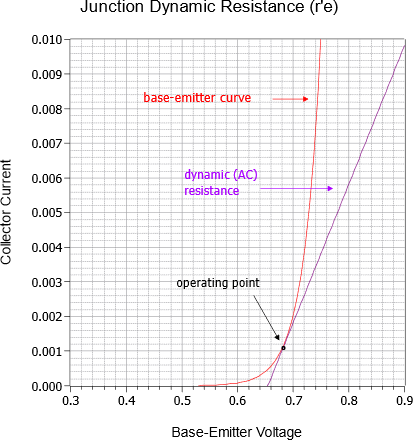
To find the dynamic resistance of the junction, first recall that the AC signal is riding on the DC bias current, as plotted in Figure 6.2.1.[1] We can imagine that the AC signal is causing this point to trace back and forth along the curve. Of course, as this is a small signal analysis, this sweep will be very small, perhaps only a few percent of the quiescent current and can be approximated as a straight line segment. The slope of this line segment represents its conductance.[2] The reciprocal of conductance is resistance; therefore, the reciprocal of the slope represents the resistance of the device. Consequently, we can approximate the dynamic resistance of the device as the reciprocal of the slope of the line tangent to the operating point (that is, the reciprocal of the slope of the line tangent to the quiescent bias current IC ). In reality, this slope is changing slightly as the signal swings back and forth along the base-emitter I-V curve. As the signal swings positive and goes above the quiescent point the slope is a little steeper producing a slight reduction in dynamic resistance. In contrast, as it swings negative, going below the quiescent point, the slope becomes a bit more shallow and produces a slightly higher resistance. As a result, we are effectively computing an average value for the dynamic resistance by assuming this is a straight line segment. The variance in this resistance will be a source of asymmetrical distortion in the amplifier of the type shown in Chapter 6, Figure 6.3.4. We shall see more on this later.
In order to derive an equation for the dynamic resistance, we begin with the Shockley equation from Chapter 2, Equation 2.2.1, slightly modified to reflect the terminal names of a BJT.
![\[I_C = I_S \left( e^{\frac{V_{BE} q}{n k T}} −1 \right) \]](https://pressbooks.nscc.ca/app/uploads/quicklatex/quicklatex.com-af7cce24fe0b62b4af7ee3234b457921_l3.png "Rendered by QuickLaTeX.com")
IC is the junction (collector) current,
IS is the reverse saturation current,
VBE is the voltage across the junction (base-emitter),
q is the charge on an electron, 1.6E−19 coulombs,
n is the quality factor (typically between 1 and 2),
k is the Boltzmann constant, 1.38E−23 joules/kelvin,
T is the temperature in kelvin.
At 300 kelvin (about 80°F), q/kT is approximately 38.6, thus for any reasonable value of VBE the “−1” term is small enough to ignore. Also, we shall take n as 1.
The equation then reduces to
![\[I_C=I_S e^{38.6V_{BE}} \]](https://pressbooks.nscc.ca/app/uploads/quicklatex/quicklatex.com-c00ded463ae04057c592337c3d36e3b1_l3.png "Rendered by QuickLaTeX.com")
(6.2.1)
To find the slope we take the first derivative of Equation 6.2.1 with respect to VBE .
![\[\frac{dI_C}{dV_{BE}} =38.6 I_S e^{38.6V_{BE}} \]](https://pressbooks.nscc.ca/app/uploads/quicklatex/quicklatex.com-53dc47f571b94ce4f8678ad246ecec5c_l3.png "Rendered by QuickLaTeX.com")
(6.2.2)
Substituting Equation 6.2.1 into Equation 6.2.2 yields
![\[\frac{dI_C}{dV_{BE}} = 38.6 I_C \]](https://pressbooks.nscc.ca/app/uploads/quicklatex/quicklatex.com-6f427c13edf8c8e280f3573b098fee7c_l3.png "Rendered by QuickLaTeX.com")
By definition, the dynamic junction resistance is the reciprocal of the slope.
![\[\frac{dV_{BE}}{dI_C} = 25.9mV I_C \} We call this <em>r</em>′ . This value is slightly low as it doesn't include bulk resistance so a good approximation is \[r'_e = \frac{26 mV}{I_C} \]](https://pressbooks.nscc.ca/app/uploads/quicklatex/quicklatex.com-6f5f27ea0c94fd0edcd053d3d9e92031_l3.png "Rendered by QuickLaTeX.com")
(6.2.3)
It is important to note that IS in Equation 6.2.2 varies with temperature. Therefore r′ varies with temperature as well, decreasing with increasing temperature. This carries important ramifications with the thermal stability of higher power amplifiers as we shall see in subsequent work.
One of the most important things to remember here is that the DC collector current sets up the resistance of the AC model. In other words, the stability of the AC circuit will depend in part on the stability of the DC bias (hence our emphasis on stable bias circuits in Chapter 5).
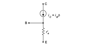
We now have our AC model, as shown in Figure 6.2.2. This is a simplified model in that it does not include junction capacitance effects, lead inductance and the like. It is appropriate, therefore, as a low to mid-band frequency model. To summarize, the AC collector current, IC , is determined by the AC input current, IB ; which is in turn a function of the the size of the applied input e signal. In contrast, r’e is set by the DC bias current, IC. The AC input can produce small variations in r’e which are manifested as waveform distortion.
Given the model, there are three ways to configure the transistor as an amplifier:
- Common Emitter. The input is applied to the base and the output is taken at the collector. The emitter terminal is at the common or ground point. This configuration exhibits both voltage gain and current gain. It also inverts the phase of the signal.
- Common Collector. The input is applied to the base and the output is taken at the emitter. The collector terminal is at the common or ground point. This configuration offers a voltage gain of about unity but does exhibit current gain. It maintains the phase of the input signal. It is also referred to as an emitter follower or voltage follower.
- Common Base. The input is applied to the emitter and the output is taken at the collector. The base terminal is at the common or ground point. This configuration exhibits voltage gain but the current gain is unity at best. It also maintains the phase of the input signal.
We shall examine each of these topologies in turn. Each of these can be made using a variety of DC bias techniques. For example, a two-supply emitter bias or voltage divider bias could be used for any of the three AC topologies, and further, they could utilize either an NPN or PNP transistor.
