1.8 An Alternate Hypothesis Regarding PN Junctions
And now for something completely different…
One of the great things about the Internet is that you can find almost anything on it. In contrast, one of the terrifying things about the Internet is that you can find almost anything on it. The following is presented in keeping with the dictum that “It must be true because I saw it on the Internet”.
An Alternate Hypothesis Regarding PN Junctions
In order to learn how to design circuits and systems using transistors and other solid state devices, students of electronics are told in their courses how semiconductors function. The atomic structure of crystalline silicon is examined in its intrinsic and doped states. Discussion of energy levels, conduction band electrons and hole production quickly follow. Soon, the student encounters the PN junction, a basic building block of modern electronics, and learns about majority and minority carriers, depletion regions, barrier potentials, leakage current and other exotica. This information is intended to explain just how solid state devices really work and it can end up sounding quite obtuse. It may sound so complicated, in fact, that the student assumes that only a genius could design such devices and relegates him or herself to a lower paying engineering or technician job. This should not be the case!
Recent investigations by Farcebook authors have uncovered some startling facts:
- Semiconductors don’t really work the way we’ve all been told. In fact, the fundamental theory is much simpler.
- This lie has been fabricated and perpetuated by the economic and political elite, a group of people with cushy, high paying jobs; jobs so easy in the light of the real theory that even CEOs, hedge fund managers, televangelists, TV psychics and other folk of nil capability could do it in their sleep (well, OK, the executives would still need an army of assistants and the televangelists would continue to be outraged by your private life, but you get the general idea). By making their jobs sound difficult these people get to sit around all day eating eclairs and reading Esquire for an eight figure annual income.
It is high time that the truth be told and this farcical sham be torn down! As an example, we shall see how a simple diode really works.
So, you think a diode is composed of semiconducting material? Think again! One of the chief researchers at Bell labs in the 1940s and 50s was a certain Doctor Schlocking. After several experiments involving solid state diodes, Dr. Schlocking wrote in his diary:
“This stuff don’t work at all. Better go back to tubes before they can me. Ooops, must let the dog out.”
Schlocking was often pestered by his dog Melvin who reminded him of a small selfpropelled dust mop, and who was approximately as clean. The diary continued:
“If only there was a way in which Melvin could let himself out. Even better…if he couldn’t get back in!”
This ominous tone led to Schlocking’s invention of the now infamous one-way doggie door that can be seen mounted to the bottom of normal doors across the country. Schlocking knew how to milk an idea and took the form to its extremes by developing the cat door, the mouse door, the grasshopper door, the flea door (an early attempt at a flea and tick collar) and even the amoeba door. This last unit when properly designed could force microscopic parasites and bacteria out of the human body and not allow them to re- enter. This was instrumental in the development of the polio vaccine, in spite of the fact that the vaccine was produced some years earlier. Schlocking’s greatest achievement, however, came when he shrunk the doggie door still further to produce the electron door. This is the fundamental unit of modern electronics.
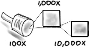
In the figure below, we see a cross section of a diode and close-ups.

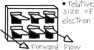
Even at 10,000X magnification we can still see nothing of the PN junction. If we go a bit further, something interesting comes into focus (see the second figure).

Yes! A PN junction is nothing more than a huge array of real tiny one-way doggie doors! Here’s how it works: Electrons are a lot like marbles. When one hits a doggie door from behind, the door flips open allowing the marble through (i.e., allowing current to flow). If the electron hits the doggie door from the front, the flap closes and the electron can’t get through (i.e., no current flow). Now obviously, if we hang the diode vertically, gravity should open all the doors and we’ll get lots of electrons (i.e., current flow) in either direction. In truth, a real diode doesn’t do this. Its operation will not matter on how the diode is oriented in space. This feature is accomplished by simply adding a small coil spring to the doggie door’s hinge, forcing it to stay shut in the face of gravity. This has the negative side effect of requiring somewhat higher energy levels from the electrons to force the door open.
This force happens to be the barrier potential of the diode! It has nothing to do with so-called depletion regions. If you were an electron, would you want to go through a place called a depletion region? Of course not! Neither would electrons. They’re not stupid, you know. In any case, the stronger the spring, the greater the barrier potential. Presently diodes are made of either silicon or germanium with barrier potentials of approximately 0.7 volts or 0.3 volts, respectively. In fact, silicon and germanium are really code words meaning strong spring and weak spring! It took a while to develop small, strong springs and this is why germanium diodes were the first ones built.
Note that spring strength also plays a role in how tightly the flap can shut thus indicating the reverse leakage current. Here again we see strong spring “silicon” units having lower leakage. Theory also indicates that leakage should increase with temperature. This effect can be seen clearly in the doggie door model. At present it is impossible to create both the frame and the door out of precisely the same material and thus two different expansion coefficients exist. Because the flap is smaller than the frame it will tend to curl away at higher temperatures allowing more electrons to sneak through the gaps. At very low temperatures the flap tends to stick to the frame in much the same fashion that your tongue or lips will stick to a metal flag pole in freezing weather (also known as the Christmas Story phenomenon).
At very high forward energy levels the flaps may be literally torn off their hinges. This high volume of electrons at high energy will yield the maximum forward current. Also, note that if the energy level is high enough in the reverse direction, either the flaps will be bent and pushed through the frames or they will start to bounce violently at resonance, allowing electrons through. These two modes are referred to as avalanche and Zener conduction, respectively. The required energy level indicates the reverse breakdown voltage.
Other fine points can be explained equally by the doggie door model, as well as bipolar and field effect transistors, IGBTs and just about everything else in the field of solid state electronics with the exception of the original 7400 series TTL logic gates which utilized an array of small, edible fungi and miniature harvester ants.
More on that in a future exposé.

