
1.2 The PN Junction
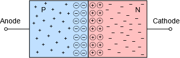
If we were to create a region of N material abutting a region of P material in a single crystal, an interesting situation occurs. Assuming the crystal is not at absolute zero, the thermal energy in the system will cause some of the free electrons in the N material to “fall” into the excess holes of the adjoining P material. This will create a region that is devoid of charge carriers (remember, electrons are the majority charge carrier in N material while holes are the majority charge carrier in P material). In other words, the area where the N and P materials abut is depleted of available electrons and holes, and thus we refer to it as a depletion region. This is depicted in Figure 1.2.1. The excess electrons of the N material are denoted by minus signs while the excess holes of the P material are denoted with plus signs. At the interface, the free electrons have recombined with holes. When an electron recombines, it leaves behind a positive ion in the N material (shown here as a circled plus sign) and produces a negative ion in the P material (shown as a circled minus sign).
We now have a region depleted of charge carriers and this will have an effect on the ability to establish a flow of current through the device. We have, in essence, created an energy hill that will need to be overcome.
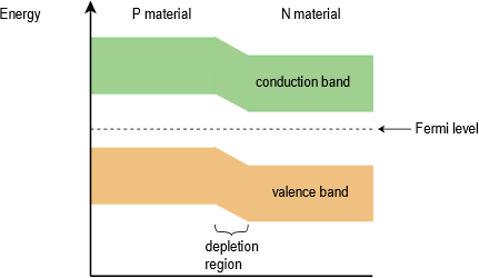
To understand the concept of the energy hill, recall that in the prior chapter it was discovered that doping an intrinsic crystal would shift the Fermi level. For N material, the Fermi level is shifted up, toward the conduction band. In contrast, for P material the Fermi level is shifted down, nearer to the valence band. When two dissimilar regions adjoin, as in the case here, the energy bands will adjust so that the Fermi levels are consistent. Effectively, this causes the bands of the P material to rise relative to the bands of the N material. The interface between the two appears as a hill, and this is the aforementioned depletion region. This situation is depicted graphically in Figure 1.2.2. Compare this energy diagram to the energy diagrams for N material and P material presented in the prior chapter. By simply aligning the Fermi levels, it should be clear how we arrive at the new energy diagram.
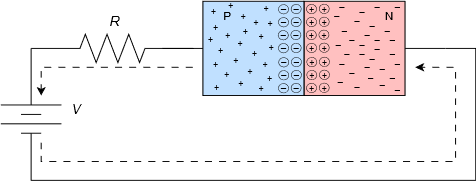
Now let’s consider what happens if we were to connect this device to an external voltage source as shown in Figure 1.2.3. Obviously, there are two ways to orient the PN junction with respect to the voltage source. This version is termed forward-bias.
Forward-Bias
The dotted line of Figure 1.2.3 shows the direction of electron flow (opposite the direction of conventional flow). First, electrons flow from the negative terminal of the battery toward the N material. In N material, the majority carriers are electrons and it is easy for these electrons to move through the N material. Upon entering the depletion region, if the supplied potential is high enough, the electrons can diffuse into the P material where there are a large number of lower energy holes. From here, the electrons can migrate through to the positive terminal of the source, completing the circuit (the resistor has been added to limit maximum current flow). The “trick” here is to assure that the supplied potential is large enough to overcome the effect of the depletion region. That is, a certain voltage will be dropped across the depletion region in order to achieve current flow. This required potential is called the barrier potential or forward voltage drop. The precise value depends on the material used. For silicon devices the barrier potential is usually estimated at around 0.7 volts. For germanium devices it is closer to 0.3 volts while LEDs may exhibit barrier potentials in the vicinity of 1.5 to 3 volts, partly depending on the color.
Another way of thinking about this is that the addition of the voltage source “flattens” the inherent energy hill of the junction. Once the applied forward-bias voltage is at least as big as the hill, current can flow easily.
Reverse-Bias
If the voltage source polarity is reversed in Figure 1.2.3, the behavior of the PN junction is altered radically. In this case, the electrons in the N material will be drawn toward the positive terminal of the source while the P material holes will be drawn toward the negative terminal, creating a small, short-lived current. This has the effect of widening the depletion region and once it reaches the supplied potential, the flow of current ceases. In essence, we have increased the size of the energy hill. Further increases in the source voltage only serve to make the situation worse. The depletion region simply expands to fill the void, so to speak. Ideally, the PN junction acts like an open circuit with an applied reverse-bias voltage.
This asymmetry in response to a supplied potential turns out to be extraordinarily useful. Perhaps the simplest of all semiconductor devices is the diode. In its basic form a diode is just a PN junction. It is a device that will allow current to pass easily in one direction but prevent current flow in the opposite direction.
Shockley Equation
We can quantify the behavior of the PN junction through the use of an equation derived by William Shockley.
![\[I = I_S \bigg(\frac {V_Dq}{e ^n^k^T} - 1\bigg)\]](https://pressbooks.nscc.ca/app/uploads/quicklatex/quicklatex.com-c322e734156b9b69402bb921b58c62ba_l3.png "Rendered by QuickLaTeX.com")
(1.2.1)
Where
I is the diode current,
IS is the reverse saturation current,
VD is the voltage across the diode,
q is the charge on an electron, 1.6E−19 coulombs,
n is the quality factor (typically between 1 and 2),
k is the Boltzmann constant, 1.38E−23 joules/kelvin,
T is the temperature in kelvin.
At 300 kelvin, q/kT is approximately 38.6. Consequently, for even very small forward (positive) voltages, the “−1” term can be ignored. Also, IS is not a constant. It increases with temperature, approximately doubling for each 10 C° rise (more on this in a moment).
If we plot the Shockley equation using typical values for a silicon device, we arrive at the curve shown in Figure 1.2.4. This plots the junction current as a function of the forward (positive) device voltage. It is a representative curve only. While all silicon diodes will exhibit this same general shape, the precise value of current for a specific voltage will vary depending on the device design.
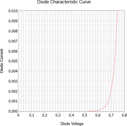
For potentials below about 0.5 volts, the current is virtually non-existent. Above this value, the current rises rapidly, becoming nearly vertical after approximately 0.7 volts. If the plot was recreated using a higher temperature, the effect would be to shift the curve to the left (i.e., a higher current for a given voltage).
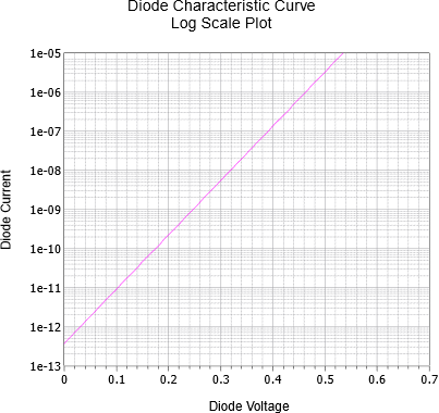
If we were to alter the graph to use a logarithmic current scale rather than a linear scale, the graph of Figure 1.2.5 results. The resulting straight line plot shows clearly the logarithmic relationship between the diode’s voltage and current.
For negative voltages (reverse-bias) the Shockley equation predicts negligible diode current. This is true up to a point. The equation does not model the effects of breakdown. When the reverse voltage is large enough, the diode will start to conduct. This is shown in Figure 1.2.6. In the first quadrant we see the same general shape we found in Figure 1.2.4. VF is the forward “knee” voltage (roughly 0.7 volts for silicon). IR is the reverse saturation current (ideally zero but in reality a very small amount of current will flow). VR is the reverse breakdown voltage. Note that the current increases rapidly once this reverse voltage is reached.
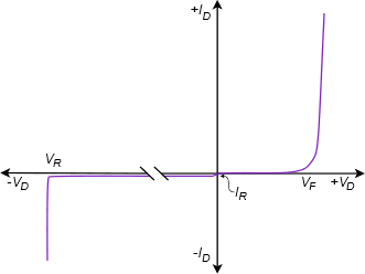
In general, diodes should not be operated in the breakdown region (the exception being Zener diodes). There are two mechanisms behind this phenomenon. The Zener effect, named after Clarence Zener, predominates when the doping levels are high and produces breakdown voltages below roughly five or six volts. It is due to the production of a very high electric field across the depletion region which then results in the production of a high current through electron tunneling. In devices using lower levels of doping, avalanche dominates. In this instance, a high electric field accelerates the free electrons to the point where they can impact surrounding atoms and create new electron-hole pairs, thus creating new free electrons that can repeat the process, resulting in a rapid increase of current.


The schematic symbol for a basic switching or rectifying diode is shown in Figure 1.2.7. This is the ANSI standard which predominates in North America. The P material is the anode while the N material is the cathode[1]. As a general rule for semiconductor schematic symbols, arrows point toward N material. In this case, the arrow also points in the direction of easy conventional current flow. Figure 1.2.8 shows an alternate schematic symbol, the IEC international standard, the difference being that it is in outline form without the body being filled in.
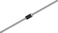
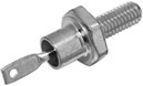
When it comes to physical device packaging, small and medium current and power devices for through-hole mounting include the DO-35 and DO-204, with the model number stamped on the body. The typical size is comparable to a 1/4 to 1/8 watt resistor. As seen in Figure 1.2.9 the cathode end is denoted by a band, reminiscent of the bar on the schematic symbol. Surface mount packages are also available. Devices handling higher currents and powers often come in stud or bolt styles such as the DO-4 shown in Figure 1.2.10. These packages facilitate mounting to a metal plate or heat sink to help dissipate the excess heat.
- Cathode is often denoted by a k. This is likely due to the word's Greek root, kathodos. ↵
