
3.7 BJT Switching and Driver Applications
As mentioned, variation in β can cause changes in collector current. This can cause performance issues. For example, when driving an LED, this can lead to variance in brightness. But what if we purposely put the transistor into saturation? Saturation is a fixed value. It is inherently stable and β no longer matters. Effectively, when a BJT saturates, β is forced to drop to whatever value is needed to produce IC(sat) . We just need to make sure that even the smallest β is large enough to cause saturation.
The Saturating Switch
A good example of this is the saturating LED driver circuit shown in Figure 3.7.1. To begin with, the whole point of the driver is to offload the current demand from the prior circuit. For example, we may wish to light an LED from the output of a logic gate or microcontroller chip. The problem is that those circuits might only be able to deliver, say, 5 mA when we might need well over 10 mA to achieve the desired brightness. The LED driver circuit is used to overcome this limitation.
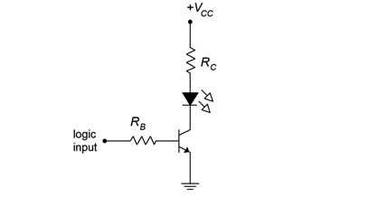
With the driver, the logic circuit will only need to supply base current, not LED current. Here is how it works: If the logic input voltage is zero, there will be no base current. This means that there will be no collector current and therefore the LED will be off. At this point the BJT is in cutoff. In contrast, when the logic level goes high, all of the logic voltage drops across RB, with the exception of VBE . This creates IB. If properly designed, this current will be sufficient to put the BJT into saturation. The BJT acts as a switch, completing the circuit between the DC supply, the LED and the current limiting resistor, RC . For this to work reliably, we have to make sure that the ratio of saturation current to base current is much less than β. A value of 10 or so would guarantee hard saturation.
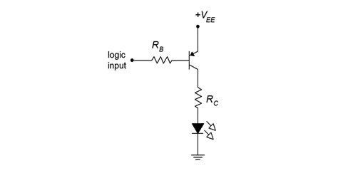
If we would like to invert the logic, that is, have a logic low turn on the LED and a logic high turn it off, we can achieve that with a PNP version of the circuit as shown in Figure 3.7.2.
Example 3.7.1
Determine the LED “on” current for the circuit of Figure 3.7.3. Assume the logic “on” voltage is 5 volts, VLED = 1.8 volts and VCE(sat) = 0 .
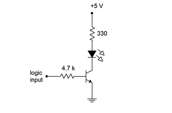
First, find the base current.
![\[I_B = \frac{V_{logic}-V_{BE}}{R_B} \]](https://pressbooks.nscc.ca/app/uploads/quicklatex/quicklatex.com-6869396b679936286bb5b83a17192018_l3.png "Rendered by QuickLaTeX.com")
![\[I_B = \frac{5 V-0.7 V}{4.7 k\Omega} \]](https://pressbooks.nscc.ca/app/uploads/quicklatex/quicklatex.com-90877fd4da93626db96fc949bdaf2cb7_l3.png "Rendered by QuickLaTeX.com")
![\[I_B = 915 \mu A \]](https://pressbooks.nscc.ca/app/uploads/quicklatex/quicklatex.com-203a9035848b73d00134c086e73907b7_l3.png "Rendered by QuickLaTeX.com")
Now find IC(sat) , making sure the BJT is in saturation. This will be the LED current.
![\[I_{C(sat)} = \frac{V_{CC}-V_{LED}}{R_C} \]](https://pressbooks.nscc.ca/app/uploads/quicklatex/quicklatex.com-64451aeacb799fb1f3a40a2d34bc5359_l3.png "Rendered by QuickLaTeX.com")
![\[I_{C(sat)} = \frac{5 V-1.8V}{330\Omega} \]](https://pressbooks.nscc.ca/app/uploads/quicklatex/quicklatex.com-023d7491edc3dcdbf344d169c23c6a56_l3.png "Rendered by QuickLaTeX.com")
![\[I_{C(sat)} = 9.7mA \]](https://pressbooks.nscc.ca/app/uploads/quicklatex/quicklatex.com-eb4f26b75e4fa5e2d5c372ed835383f9_l3.png "Rendered by QuickLaTeX.com")
The ratio of these two currents is just over 10:1. This will guarantee hard saturation.
There are many different applications for saturating switches. Just about anywhere you can imagine a relay being used, you can consider a transistor switch. The transistor switch has the advantages of small size, no moving parts to wear out and very fast switching speeds. Relays have the advantage for very high currents. Figure 3.7.4 shows an example of direct motor drive using a saturating BJT switch.
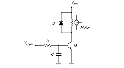
This circuit is used to control the speed of a DC motor through a technique called pulse width modulation. The speed of the motor will depend on the average voltage applied to it. The trick here is that instead of applying a continuously variable voltage to the motor, we instead apply a series of pulses of varying width. These pulses are sufficient to saturate the BJT, causing it to behave as a switch. These pulses are so fast that the motor does not start and stop, but rather inertia keeps it going. Instead, the motor responds to the averaged value of these pulses. If the pulses are narrow and widely spaced, the average value will be low and the motor speed will be slow. If the pulses are wide and closely spaced, the average will high and the motor speed will be fast.
The resistor and capacitor at the base are used to shape the incoming pulse to improve performance. The diode across the motor winding is particularly important. It is referred to as a snubbing diode.[1] Without it, the switching transistor might experience large and damaging transient spikes. Here’s why: Let’s assume the BJT is on and conducting fully. This current is the same current flowing through the motor’s armature, which is little more than a huge coil of wire. That means it exhibits a lot of inductance.
When we turn off the transistor, we are attempting to turn off the armature current, but the current through an inductor cannot change instantaneously. The result is that the winding now generates a large flyback voltage (also called an “inductive kick”) directly across the BJT. That is, the winding momentarily appears as a high voltage source of opposite polarity and, via KVL, this potential appears from collector to emitter. This could damage the BJT. The snubbing diode effectively short-circuits the winding when it reverses voltage polarity, preventing the large spike. The remainder of the time the diode is reverse-biased and effectively out of the circuit.
The Non-Saturating Driver
It is also possible to create a switch or driver that is non-saturating. An example of a non-saturating LED driver is shown in Figure 3.7.5
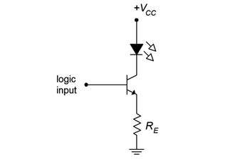
The advantage of this circuit is that it requires less current from the logic circuit. Unfortunately, it also exhibits higher transistor power dissipation and requires a DC source that is higher than the logic level. The operation is as follows: As in the saturating driver, if the logic level is zero, there is no rise in the base-emitter loop and the collector current will also be zero. With a high logic voltage, via KVL around the base-emitter loop, all of the logic input voltage drops across RE, with the exception of VBE . This creates IE which is virtually the same as IC (which is ILED ).
This circuit “programs” the emitter current via the resistor and logic voltage. Therefore it is fixed and stable. This process is sometimes referred to as bootstrapping. It might be said that the emitter voltage is “bootstrapped” to within 0.7 volts of the logic input level, keeping it stable.[2] In any case, if β varies, this will cause an inverse change in IB with no change in IC . A negative logic PNP version is also possible and left as an exercise.
Example 3.7.2
Determine the LED “on” current for the circuit of Figure 3.7.6. Assume the logic “on” voltage is 5 volts, VLED = 1.8 volts and β = 100.
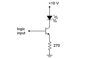
We can find IC directly because IC ≈ IE . This will be the LED current.
![\[I_C = \frac{V_{logic}-V_{BE}}{R_E} \]](https://pressbooks.nscc.ca/app/uploads/quicklatex/quicklatex.com-ff2ea9984513cff4099752ac88b8492a_l3.png "Rendered by QuickLaTeX.com")
![\[I_C = \frac{5V−0.7V}{270\Omega} \]](https://pressbooks.nscc.ca/app/uploads/quicklatex/quicklatex.com-ed137c67dfff345a6c636291e3ef0826_l3.png "Rendered by QuickLaTeX.com")
![\[I_C = 15.9 mA \]](https://pressbooks.nscc.ca/app/uploads/quicklatex/quicklatex.com-d9f8d04c0b491f0f26dd0176f75abce8_l3.png "Rendered by QuickLaTeX.com")
Note that β was not used. All it tells us is that IB = 15.9 mA/100, or 159 μA. A higher β would simply lead to a lower base current.
For the sake of completeness, we might also note that
![\[V_{CE} = V_{CC}-V_{LED}-V_{RE} \]](https://pressbooks.nscc.ca/app/uploads/quicklatex/quicklatex.com-5d62c55aba5f176212e510b9720c8e07_l3.png "Rendered by QuickLaTeX.com")
![\[V_{CE} = 10 V-1.8V-4.3 V \]](https://pressbooks.nscc.ca/app/uploads/quicklatex/quicklatex.com-bdae99b2b3fced68ed25878152127d47_l3.png "Rendered by QuickLaTeX.com")
![\[V_{CE} = 3.9V \]](https://pressbooks.nscc.ca/app/uploads/quicklatex/quicklatex.com-c0eeb6714a6f1b01155a48cde5975e2b_l3.png "Rendered by QuickLaTeX.com")
Clearly, if VCE is 3.9 volts, the transistor is not in saturation.
3.7.3: The Zener Follower
In the prior chapter we examined a method of regulating the output voltage of a filtered full-wave rectifier through the use of a Zener diode. The downfall of that specific circuit is that it was not particularly efficient because it drew a fair amount of current even when the demand for load current was light. Using the concept of locking one voltage to another, as in the non-saturating switch, we can create a nice improvement, the Zener Follower.
A Zener Follower is shown in Figure 3.7.7. The input signal is the positive rectified and filtered output of the AC-to-DC power supply.
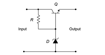
The primary thing to notice is that the Zener diode is reverse-biased via resistor R. That is, a current will flow down through R and into the Zener. The Zener presents a fixed potential, VZ . Consequently, the difference between the input voltage and VZ must drop across R, and by extension, VCB . Further, the final output voltage is the voltage at the BJT’s emitter which must be VZ − VBE . As these are both fixed, stable potentials, the output must likewise be a fixed, stable voltage. Lastly, because VCE = VCB + VBE , it is apparent that any variation between the input voltage and the desired output (for example, due to ripple) must be dropped across the BJT.
The diode current is kept low in the Zener Follower and thus its power dissipation is also modest. Further, current draw from the input circuit is a direct reflection of load current demand. If the load current requirement is low, very little current will flow through the transistor, and ultimately, from the input circuit. This makes for a more efficient system.
- It is also known as a commutating diode, clamp diode, flyback diode and by a host of other names. But as Shakespeare said, “A snubbing diode by any other name would clamp a flyback voltage as well”. Or something like that. ↵
- This is in reference to the old phrase “pulling yourself up by your bootstraps”. To be honest, that saying never made sense to this author and all that ever happened when I tried to do it was that my arms got tired. ↵
