2.4 Clampers
A clamper is circuit that adds a DC offset to an AC signal in such a way that the resulting voltage is uni-polar. A positive clamper adds a positive offset such that the former negative peak now sits at zero volts. In like fashion, a negative clamper adds in a negative offset such that the former positive peak now sits at zero volts. Clampers are also referred to as DC restorers. Clampers can also be biased so that the new peak point is something other than zero volts.
The concept of a clamper is fairly simple; we just add a DC voltage to the existing AC signal. The trick is in getting the circuit to automatically determine what the DC shift needs to be. This way, if the amplitude of the input signal changes, the offset can track with it.
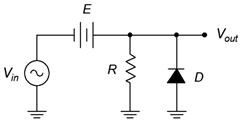
First, let’s consider the prototype circuit in Figure 2.4.1. This is a fixed DC offset circuit. The DC source E adds a positive offset to the input signal. If the offset is equal to the peak value of the input, the negative peak will rise up to zero volts and the diode will never turn on (meaning that it will not load the input and change the wave shape).
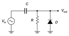
In Figure 2.4.2 the fixed DC source has been replaced with a capacitor. This capacitor is used to create the DC offset. Unlike the fixed source, the capacitor voltage will vary with the peak value of the input and therefore precisely compensate to produce an ideally clamped output signal. As long as the time constant for this capacitor and the surrounding resistance is much longer than the period of the input waveform, it will achieve proper clamping action.
Here is how the circuit operates. For the initial positive cycle, the capacitor is uncharged and the diode is reverse-biased. As the RC time constant is much longer than the input period, the output voltage merely follows the input voltage. Once the input signal swings negative, the diode turns on. This bypasses the parallel resistor and drastically reduces the charge time constant. This means that the capacitor voltage will begin to track the negative portion of the input signal while the output stays near zero volts. Note that the capacitor voltage will have a polarity of minus-to-plus from left to right, in keeping with Kirchhoff’s voltage law. The capacitor voltage will track the negative input voltage all the way down to the negative peak. Once the input begins to reverse slope and rise toward zero, the diode will be turned off due to the potential now held on the capacitor. At this point, the capacitor has a voltage across it that is equivalent to the negative peak value of the input signal and it will behave just like the fixed DC voltage source in the prototype. The input is just now starting to track in the positive direction from its negative peak while the capacitor holds this same magnitude of voltage. The result is that the output is at zero volts and as the input continues to swing positive, the output will track it, thus producing the desired level shift.
Of course, circuits are never perfect. First, the forward voltage drop of the diode will result in a negative peak that’s not precisely at zero volts but is instead about −0.7 volts. Second, it may take more than one cycle of the input to “grab” the peak value, all depending on the period and the precise charge and discharge time constants. As you might guess, flipping the polarity of the diode will result in a negative clamper instead of a positive clamper. Also, if we add a DC source in series with the diode, like we did with the biased clipper, we can create a biased clamper. This is shown in Figure 2.4.3.
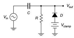
Example 2.4.1
![]()
![]()
![]()
Computer Simulation
To verify the analysis of Example 2.4.1, the circuit is captured as shown in Figure 2.4.4. A common 1N914 switching diode is used.
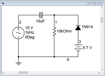
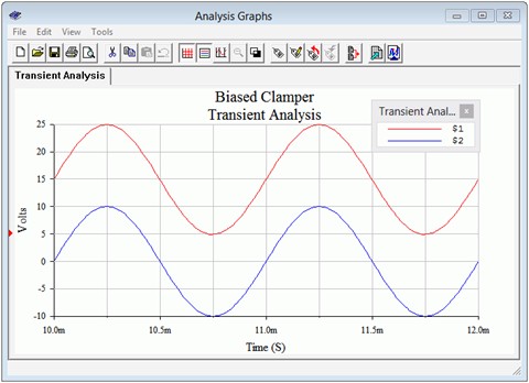
The transient analysis is shown in Figure 2.4.5 and is precisely as predicted. The input waveform is blue and the clamped output is shown in red. The analysis was delayed ten milliseconds in order to get past the initial charge phase and observe the steady state operation.

