6.4 Common Collector Amplifier
The common collector amplifier is often referred to as an emitter follower, or more generically, as a voltage follower. The key characteristics of a voltage follower are a high input impedance, a low output impedance and a non-inverting voltage gain of approximately one. The name comes from the fact that output voltage follows the input, that is, it’s at the same voltage level and is in phase with the input. While this configuration does not produce voltage gain, it does produce current gain, and therefore, power gain. It’s primary purpose is to reduce impedance loading effects, for example, to match a high impedance source to a low impedance load. Consequently, they are used as high-Z input buffer stages or as drivers for low impedance loads such as loudspeakers.
A common collector amplifier using two-supply emitter bias is shown in Figure 6.4.1. The input is coupled into the base like the common emitter amplifier, however, the output signal is taken at the emitter instead of at the collector. Because the collector is at the AC common, there is no need for a collector resistor.
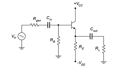
Perhaps the best way to think about the follower is not that it gives a voltage gain of one, but that it will prevent signal loss. The analysis follows, using Figure 6.4.2.
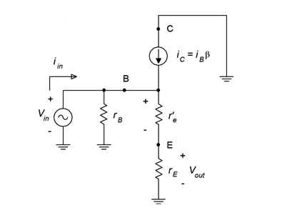
First, the AC emitter resistance, rE , is either the emitter bias resistor, RE, or the parallel combination of RE
and the load resistance, RL. We’ll use the former in order to determine the unloaded gain and the latter to determine the loaded gain, similar to what we did with the common emitter amplifier concerning RC and RL. The AC base resistance, rB, typically boils down to the base biasing resistor just as we saw with the common emitter amplifier (RB in a two-supply emitter bias or R1||R2 for a voltage divider bias).
Voltage Gain
The derivation for the emitter follower’s voltage gain equation is similar to that shown for the common emitter amplifier. We begin with the basic definition of voltage gain and then expand using Ohm’s law.
![]()
![]()
![]()
(6.4.1)
This equation is very similar to that of Equation 7.3.1. Here we see that the output signal is in phase with the input and that if rE ≫ r′e, the gain approaches unity. Signal distortion tends to be low in followers because a gain of one is a desired goal.
Input Impedance
The derivation for Zin and Zin(base) are unchanged compared to the common emitter configuration. The formulas are repeated below for convenience.
![]()
![]()
Output Impedance
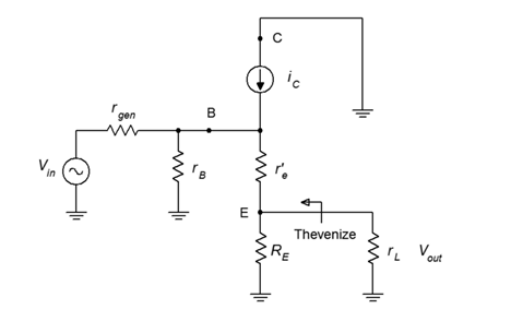
The derivation for common collector output impedance varies considerably from that of the common emitter. We shall use Figure xx for the analysis.
First, note that this diagram splits the AC emitter resistance into its two components, RL and the biasing resistor RE. This is because we want to find the effective resistance of the source that drives the load, so logically we can’t include the load in that value. We begin by looking back into the emitter from the perspective of the load. We see the emitter bias resistor in parallel with whatever the impedance is looking back into the emitter terminal.
![]()
(6.4.2)
Zout(emitter) is equal to r′e in series with the equivalent resistance of the network above it and to the left. The internal resistance of e the current source is high enough to ignore so we’re left with the equivalent resistance looking back off the base. We’ll call this ZB(equivalent) . At first glance this might appear to be the parallel combination of rgen and rB, but this ignores the effect of the e collector current source. What we really want is the effective resistance as seen from the perspective of r′ , not as seen from the base terminal.
![]()
(6.4.3)
![]()
![]()
![]()
6.4.4)
Combining Equations 6.4.2, 6.4.3 and 6.4.4 yields
![]()
(6.4.5)
In many instances the emitter bias resistor is large enough to ignore.
Example 6.4.1
For the follower shown in Figure 6.4.4, determine the input impedance, output impedance and load voltage. Assume β = 100 and Vin = 100 mV.
First, find IC in order to find r′ . Assuming an unloaded divider, V will equal half of the DC supply, or 10 volts. We lose 0.7 volts across the base-emitter junction leaving 9.3 volts across the 10 kΩ. This results in a collector current of 930 μA and an r′e of 28 Ω.
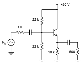
To find Zin
![]()
![]()
![]()
![]()
![]()
![]()
This value is not particularly high when compared with the rather large source resistance of 1 kΩ. There will be some signal loss here due to the voltage divider effect between the two impedances. And now for Zout
![]()
![]()
![]()
This value is much, much lower than anything we saw with the common emitter amplifiers. Therefore this circuit can drive much lower impedance loads with minimal signal loss. The loaded gain from base to emitter is
![]()
![]()
![]()
As mentioned, we need to include the effect of the 1 kΩ source impedance. This will create a voltage divider with the input impedance.
![]()
![]()
![]()
![]()
![]()
![]()
Finally, we get to the load voltage.
![]()
![]()
![]()
At this point the question might be, “Why did we go to the trouble of building this circuit when we lost 15% of the input signal?” Well, consider what would have happened without the circuit. If we had connected the source directly to the load, the resulting 1 kΩ/500 Ω voltage divider would have dropped the load voltage to 33 mV. This circuit prevented that loss.
A High Impedance Source: The Guitar Pickup
In Example 6.4.1, the source had an internal impedance of 1 kΩ, much higher than we would see with, say, a laboratory function generator (probably 50 Ω). Things could be much worse. Consider the electric guitar pickup. The job of a pickup is to transform the vibrations of the guitar strings into an electrical signal so that it can be amplified. It is commonly thought that a pickup is some form of microphone but this is not true.
A guitar pickup is little more than a magnet surrounded by numerous turns of fine wire, as shown in Figure 6.4.5. This particular pickup is for a bass guitar but the construction is similar for all types of guitars and basses.
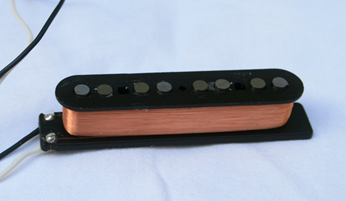
Here is it how works: The magnet creates a field around the guitar strings. Because the strings are steel, their reluctance is much less than the surrounding air, therefore, they distort or bend the magnetic field. When a string is plucked, the field moves back and forth along with it. As the field moves, the flux lines cut across the coil’s wire and this action induces a current in the conductor in accordance with Faraday’s Law of Induction. This current is then fed to the amplifier.
A typical guitar pickup consists of perhaps 5000 turns of very fine wire, 42 AWG being typical. 42 gauge copper wire has a resistance of around 1.6 Ω per foot so the DC resistance of the coil can be over 5 kΩ. Further, that many turns of wire around a magnet can produce a very large inductance, perhaps several henries, that is in series with this resistance. There is also distributed capacitance and cable capacitance in parallel that could be upwards of 1 nF. The result is a complex impedance with resonance effects, regions of which can be tens of kΩ in magnitude. What makes this more challenging is that because the impedance is a function of frequency, the voltage divider effect with the amplifier’s input impedance also becomes a function of frequency. For example, the increasing impedance due to XL will result in increasing attenuation with frequency. This is akin to turning down the treble on the amplifier. Generally, not a good result. How do we limit this effect? Simple. We make a circuit with a very, very high input impedance. How do we do that? Well, there are several ways, including the use of field effect transistors and operational amplifiers, but we can also obtain high input impedances through the use of a dual BJT configuration called the Darlington pair.
The Darlington Pair
The Darlington pair was invented by Sidney Darlington, an American engineer. The configuration leads to a compound device with a very high β. Used properly, this can lead to amplifier circuits with very high input impedance. A Darlington pair is shown in Figure 6.4.6.
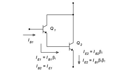
The operation is as follows. The base current of the first transistor, Q1, is multiplied by the β of Q1 resulting in Q1‘s emitter current. This current is fed into the base of the second transistor, Q2, where it is multiplied by the β of Q2 resulting in Q2‘s emitter current. If we treat the pair as a single device, then the effective β of the pair is β1β2 . Given typical values for β, the compound value can be in the vicinity of 5000 to 10,000. The functional downside to this arrangement is that VBE is now doubled to 1.4 volts (for silicon) and the effective r′e of the pair is doubled as well. These issues are minor when compared to the advantage of the huge current gain that can be obtained. The bottom line when using a Darlington pair is to treat it like an ordinary transistor except that it has a very large β and both VBE and r′e are doubled compared to the ordinary values.
Example 6.4.2
Determine the output voltage for the follower shown in Figure 6.4.7. Assume the input is 100 mV peak and the β for the Darlington pair is 10,000.
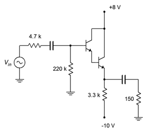
The first thing that might look a little odd, at least compared to previous bias circuits, is that the base biasing resistor is so much larger than the emitter biasing resistor. Normally, this would lead to an unstable Q point but that’s not a problem here. Because β is so large, RB can be much larger than normal and we’ll still achieve good stability. In fact, we can still use the approximation that the base is at DC ground. This being true, the analysis proceeds as follows
![]()
![]()
![]()
![]()
![]()
![]()
![]()
![]()
![]()
This value is in parallel with the base biasing resistor, creating the input impedance.
![]()
![]()
![]()
This is much higher than we have seen in previous circuits. The loaded gain from base to emitter is
![]()
![]()
![]()
Now to include the effect of the 4.7 kΩ source impedance. This will create a voltage divider with the input impedance, minimal as it turns out.
![]()
![]()
![]()
![]()
![]()
![]()
The load voltage is
![]()
![]()
![]()
If we had connected the source directly to the load, the 4.7 kΩ/150 Ω divider would have squashed the applied signal into a shadow of its former size, leaving us with just 3 mV.
Computer Simulation
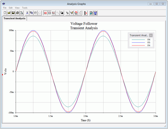
To verify the results of Example 6.4.2, we’ll run a transient analysis. The input schematic is shown in Figure 6.4.8.
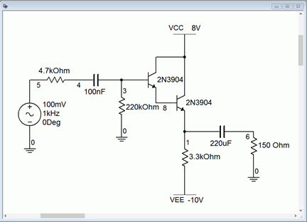
Of interest here will be the voltages at the source, base and load. As the input impedance/source impedance divider was 0.976, we expect 97.6 mV at node 4. At the output, node 6, we expect to see our final computed value of 86 mV. The output plot of the simulation is shown in Figure 6.4.9. The simulation concurs.
The Phase Splitter
Figure 6.4.10: A simple phase splitter.A phase splitter is a combination of a common emitter amplifier and a common collector follower using a single transistor. The purpose of the circuit is to produce two versions of the input signal: a buffered version identical to the input and an inverted version, both waves having the same amplitude. The circuit is used for differential line driver systems. This scheme helps to minimize outside noise and interference picked up by communications cables. There are other ways to create phase splitters, including using differential amplifiers or op amps, but this BJT-based version is a minimalist solution.[1] The basic circuit is shown in Figure 6.4.10.
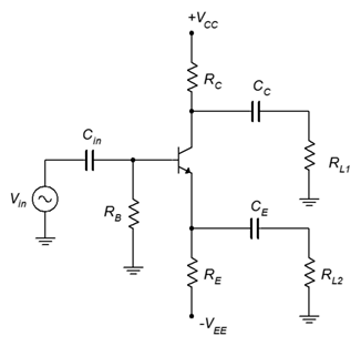
For proper operation, the circuit is largely symmetrical. That is, RL1 = RL2 , RE = RC , and CC = CE . That being the case, the AC collector and emitter resistances will be equal (rC = rE ). If we then look at the basic gain equations, we find that both loads will receive the same gain magnitude (just under unity), although RL1 will see the signal inverted.
![]()
![]()
- For details on alternate methods, see Fiore, J, Operational Amplifiers and Linear Integrated Circuits: Theory and Application, another free OER text. ↵

