3.5 Ebers-Moll Model
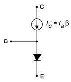
A good, functional model of the BJT is the simplified Ebers-Moll model shown in Figure 3.5.1. This utilizes an ideal diode to model the base-emitter junction and a current-controlled current source located at the collector-base. This model is sufficient to achieve good analysis results with a variety of DC and low frequency circuits. It is important to remember, though, that β varies not only from device to device, but also varies with changes in temperature, collector current and collector-emitter voltage.

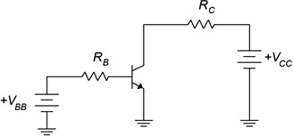
We can put the Ebers-Moll model to use in basic DC biasing circuits. To properly bias the BJT we need to make the collector-base reverse-biased and the base-emitter forward-biased. In other words, VC > VB > VE . There are many ways to achieve this. One method places the emitter at ground, a modest DC source in the base-emitter loop, and a somewhat higher DC source at the collector. An example is shown in Figure 3.5.2.

The two resistors serve to limit the transistor’s currents and voltages. Because the emitter is at ground, the common point, this circuit is classified as having a common emitter configuration. There are many possible common emitter circuits. We shall refer to this one specifically as base bias.
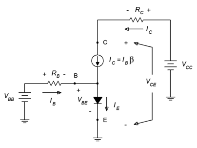
Now, let’s replace the transistor with the Ebers-Moll model. The result, with added voltage polarities and current directions, is shown in Figure 3.5.3.

Given values for the resistors, power supplies and β, all of the currents and voltages may be determined using fundamental circuit analysis techniques. The basic idea is to create KVL equations for the two loops and then expand using Ohm’s law. We begin with the base-emitter loop.
![]()
![]()
![]()
(3.5.1)
And for the collector-emitter loop:
![]()
![]()
![]()
(3.5.2)
To obtain IC , recall that IC = βIB .
Example 3.5.1
![]()
![]()
![]()
![]()
![]()
![]()
![]()
![]()
![]()
The preceding example illustrates that the place to start the analysis is in the base-emitter loop instead of the collector-emitter loop. This is because in the base-emitter loop we have the forward-biased base-emitter junction which has a known potential (approximately 0.7 volts). In contrast, the collector-emitter voltage is an unknown as it includes the reverse-biased collector-base junction. That voltage will depend on other circuit elements, most notably the collector resistor and associated supply.
An improvement on the circuit of Example 3.5.1 would be to redesign it for a single power supply rather than two supplies. This is easy to do. All that is needed is to keep the base current unchanged. If that remains at its original value then the collector current won’t change and consequently nothing in the collector-emitter loop will change either. Using the 15 volt source for VBB means that the voltage across RB will increase to 14.3 volts. Ohm’s law then indicates that RB must be 14.3 volts divided by 46.5 μA, or 307.5 kΩ.
β Variation Issues
There is a major problem with the circuit of Figure 3.5.2, namely, it lacks stability of collector current and collector-emitter voltage. As we shall see in upcoming chapters, it is important to keep these parameters stable in order to ensure consistent performance for many kinds of circuits. As we noted from our inspection of the 2N3904 data sheet, the variation of β can be quite large at a given operating point. If we also add in the variance due to temperature and other factors, we may be looking at a 10:1 range. If we repeat Example 3.5.1 with a doubled β of 200, the base-emitter loop is unchanged but the collector current doubles to 9.3 mA. This increases the voltage drop across RC to 9.3 volts which then forces VCE to drop to 5.7 volts.
Given a typical production run of transistors, this circuit might exhibit collector currents from less than 4 mA to more than 10 mA. In some applications this variation in current might be tolerable but not in all of them. For example, suppose an LED is placed in series with RC . Because the brightness of an LED depends on its current level, the brightness will now depend on the β of the specific BJT used. If this is one LED in a larger display made up of similar circuits, then the illumination will be uneven between them causing the entire display to appear off kilter.
In fact, if this circuit was built in the lab, it is quite likely that after turning on the power, you could watch IC slowly rise on your ammeter. This is because the BJT will begin to warm up as it dissipates power. As noted from the data sheet, β increases with increasing temperature. Because IB is a fixed value, any rise in β means that IC must also rise. This increased current will tend to cause a further rise in power dissipation and temperature which causes a further increase in β, and the process cycles. We have created an inadvertent thermal positive feedback loop. Left unchecked, devices could overheat and be destroyed. We will examine biasing circuits that achieve high stability in the next chapter.
There is another interesting aspect to this circuit. As noted, if we substituted the original BJT with another unit that had a higher β, the collector current would rise. What if we continued this to higher and higher β values? For example, if we increased β to 400 (admittedly, rather high) the new collector current would seem to jump up to 46.5 μA 400, or 18.6 mA. There is a “small” problem with this value. Ohm’s law indicates that this current would develop a drop of 18.6 volts across the 1 kΩ RC but that’s impossible because VCC is only 15 volts. The only way that “works” is if somehow the BJT is transformed magically into a 3.6 volt battery. No amount of prayer or letters to Santa will make that happen.[1]
- Both being equally effective. ↵

