
21 Class A Power Analysis
Learning Objective
Theory Overview
The maximum output signal, or compliance, of a class A amplifier is determined by its AC load line. The maximum peak level is determined by the smaller of VCEQ and ICQ ∙ rLoad. If either of these levels is hit, the output signal will begin to clip causing greatly increased distortion. Knowing this voltage and the load resistance, the maximum load power may be determined. Dividing this power by the total supplied DC power will yield the efficiency. The maximum theoretical efficiency of an RC coupled class A amplifier is 25% although real-world circuits may be far less. In fact, the power dissipation of the transistor itself (PDQ) may be greater than the maximum load power, clearly not a desirable condition. Note that the total supplied power is the product of the total supplied voltage and the average total current. In a class A amplifier that is not clipping, the average supplied current is equal to the quiescent DC current. In the case of a dual supply emitter biased circuit, this is simply the collector current and can be measured with a DC ammeter.
Equipment
| (1) Dual adjustable DC power supply | model: | srn: |
| (1) DMM | model: | srn: |
| (1) Dual channel oscilloscope | model: | srn: |
| (1) Low distortion function generator | model: | srn: |
| (1) Distortion analyzer | model: | srn: |
| (2) Small signal transistors (2N3904) | ||
| (1) 100 Ω resistor ¼ watt | actual: | |
| (1) 1 Ω resistor ¼ watt | actual: | |
| (1) 47 Ω resistor ¼ watt | actual: | |
| (1) 470 µF capacitor | actual: | |
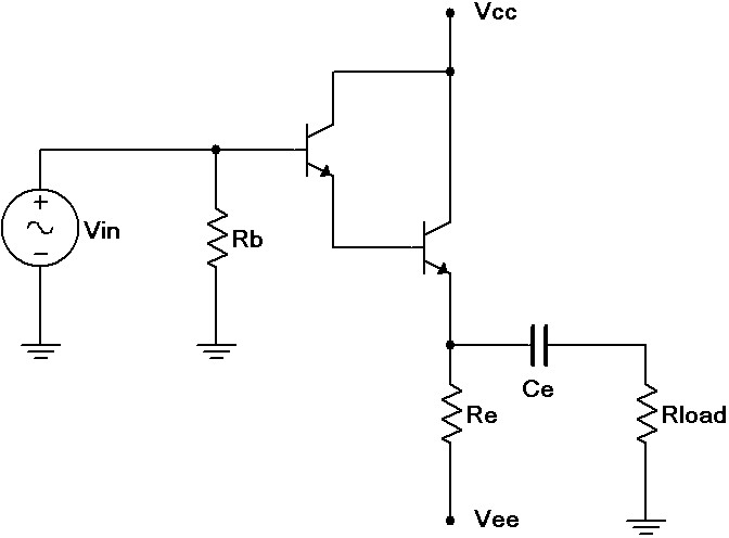
Schematic
Procedure
AC Load Line and Power Analysis
- Consider the circuit of Figure 1 using Vcc = 5 volts, Vee = −12 volts, Rb = 47 kΩ, Re = 1 kΩ, Rload = 100 Ω and Ce = 470 µF. Determine the theoretical ICQ, VCEQ, vCE(cutoff) and iC(sat), and record these in Table 1. It is helpful to plot the AC load line for step three. Note that the collector-emitter saturation voltage for a Darlington pair cannot be assumed to be 0 volts, and may be closer to one volt, thus reducing the expecting voltage swing toward the saturation point. It is also worth noting that this amplifier has a direct coupled input (i.e., no input capacitor is required due to the very small DC base voltage).
- Build the circuit of Figure 1 using Vcc = 5 volts, Vee = −12 volts, Rb = 47 kΩ, Re = 1 kΩ, Rload=100 Ω and Ce = 470 µF. Disconnect the signal source and measure the DC transistor voltages to ensure the circuit is biased correctly. Record VCEQ and ICQ in Table 1 (Experimental).
- Based on the data recorded in Table 1, determine the theoretical maximum unclipped load voltage (compliance) and record it in Table 2. Based on this, determine the maximum load power and record it Table 2 as well. Also determine and record the expected values for the quiescent power dissipation of the transistor (PDQ), the supplied DC current and power, and the resulting efficiency.
- Using a 1 kHz sine wave setting, apply the signal source to the amplifier and adjust it to achieve a load voltage that just begins to clip. Reduce the amplitude slightly to produce a clean, unclipped wave. Record this level as the experimental compliance in Table 2. From this, determine and record the experimental maximum load power. Also, capture an image of the oscilloscope display.
- Insert an ammeter in the collector and measure the resulting current with the signal still set for maximum unclipped output. Record this in Table 2 as Isupplied (Experimental).
- Using the data already recorded, determine and record the experimental PDQ, PSupplied, and η. Finally, determine the deviations for Table 2.
Clipping and Distortion
- Increase the signal until both peaks begin to clip. Record these clipping levels in Table 3. Make sure the oscilloscope is DC coupled for this measurement as any offset is important. Compare these peaks to those predicted by the AC load line. Also, capture an image of the oscilloscope display.
- Decrease the signal level so that it is about 90% of the maximum unclipped level. Set the distortion analyzer to 1 kHz and % total harmonic distortion (% THD). Apply it across the load and record the resulting reading in Table 4 (Normal). Increase the signal by about 20% so that one of the peaks is obviously clipped and take a second distortion reading, recording it Table 4 (Clipped).
Computer Simulation
- Build the circuit in a simulator and run a Transient Analysis. Use a 1 kHz 7 volt peak sine for the source. Inspect the voltage at the load. Record the peak clip points in Table 5. Reduce the input signal so that clipping disappears. Run the Distortion or Fourier Analysis at the load and record the resulting THD value in Table 5.
Data Tables
| Theory | Experimental | |
|---|---|---|
| ICQ | ||
| VCEQ | ||
| iC(sat) | X | |
| vCE(cutoff) | X |
| Theory | Experimental | % Deviation | |
|---|---|---|---|
| Compliance | |||
| PLoad(max) | |||
| ISupplied | |||
| PDQ | |||
| PSupplied | |||
| η |
| Positive Clip | |
| Negative Clip |
| %THD Normal | |
| %THD Clipped |
| Positive Clip | Negative Clip | % Distortion |
Questions
Does the maximum load power compare favorably to the supplied DC power and the transistor’s power dissipation? That is, is the circuit efficient?
How does the THD level of the clipped signal compare to that of the unclipped signal?
How well do the clip levels measured and simulated compare to the predicted AC load line?
How would the circuit performance change if a Darlington pair had not been used? Would this affect the AC load line?
Would increasing the Vcc supply increase the output compliance? Why/why not?
