
24 JFET Bias
Learning Objective
Theory Overview
Unlike bipolar junction transistors, FETs do not have a fixed forward biased junction potential. This makes bias analysis a little trickier. It is often useful to have a couple of device parameters on hand, namely IDSS and VGS(OFF). As is the case with BJTs, finding the main current (ID) is the key to finding all other circuit currents and voltages. One convenient aspect of JFETs is that the gate current can be ignored for most bias applications. Self Bias may be analyzed through the use of a Self Bias curve or through an iterative process of estimation of VGS leading to drain currents via Ohm’s law and the general FET transconductance equation. Self Bias tends to have modestly stable Q points. Source Bias is an improvement over Self Bias. It tends to swamp out VGS variation via the addition of a negative source bias voltage. This topology also turns out potentially to have a very stable transconductance although it is not examined in this exercise. Finally, Current Source Bias utilizes a BJT to establish a very stable drain current. This turns out this comes at the expense of a stable VGS and transconductance (again, not examined here), so this form of bias is not necessarily the best choice for all applications.
Equipment
| (1) Dual adjustable DC power supply | model: | srn: |
| (1) DMM | model: | srn: |
| (3) Small signal JFETs (MPF102) | ||
| (1) Small signal BJT (2N3904) | ||
| (1) 2.2 k Ω resistor ¼ watt | actual: | |
| (2) 4.7 k Ω resistor ¼ watt | actual: | |
| (1) 330 k Ω resistor ¼ watt | actual: | |
Link
Download the datasheet:
Schematics
Procedure
Determining IDSS and VGS(OFF)
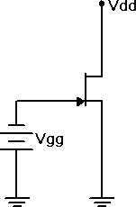
- Consider the circuit of Figure 1 using Vdd = 15 volts and Vgg = 0 volts. With nothing else in the circuit, the resulting drain current should equal IDSS. Similarly, if Vgg is gradually changed to a value negative enough to drop the drain current to zero, Vgg must be equal to VGS(OFF).
- Build the circuit of Figure 1 using Vdd = 15 volts and Vgg = 0 volts. Insert an ammeter in the drain and record the resulting current in Table 1. Slowly increase the magnitude of Vgg (i.e., make it more negative) until the drain current drops to zero (as a practical point, try to get it under 10 µA, or as low as the ammeter will allow). Record this voltage in Table 1. Repeat this process for the other two transistors. Be sure not to confuse the JFETs. Keep them in order.
Self Bias
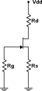
- Consider the circuit of Figure 2 using Vdd = 15 volts, Rg = 330 kΩ, Rd = 4.7 kΩ, and Rs =2.2 kΩ. Using the values of Table 1, calculate and record the expected voltages for JFET 1 in Table 2. Also record the expected drain current in Table 3.
- Build the circuit of Figure 2 using Vdd = 15 volts, Rg = 330 kΩ, Rd = 4.7 kΩ, and Rs = 2.2 kΩ. Measure and record the voltages for JFET 1 in Table 2. Based on VD, compute and record the experimental drain current in Table 3. Also determine and record the drain current deviation.
- Repeat steps 2 and 3 for the second and third JFETs.
Source Bias
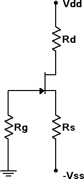
- Consider the circuit of Figure 3 using Vdd = 15 volts, Vss = −3 volts, Rd = Rs = 4.7 kΩ and Rg = 330 kΩ. A reasonable approximation for VGS in this circuit is −2 volts DC. Based on this, calculate and record the expected voltages for JFET 1 in Table 4. Also record the expected drain current in Table 5.
- Build the circuit of Figure 3 using Vdd = 15 volts, Vss = −3 volts, Rd = Rs = 4.7 kΩ and Rg = 330 kΩ. Measure and record the voltages for JFET 1 in Table 4. Based on VD, compute and record the experimental drain current in Table 4. Also find and record the drain current deviation.
- Repeat steps 5 and 6 for the second and third JFETs.
Current Source Bias
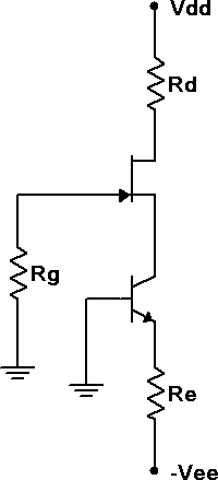
- Consider the circuit of Figure 4 using Vdd = 15 volts, Vee = −5 volts, Rd = Re = 4.7 kΩ and Rg = 330kΩ. Calculate and record the expected voltages for JFET 1 in Table 6. Also record the expected drain current in Table 7.
- Build the circuit of Figure 4 using Vdd = 15 volts, Vee = −5 volts, Rd = Re = 4.7 kΩ and Rg = 330 kΩ. Measure and record the voltages for JFET 1 in Table 6. Based on VD, compute and record the experimental drain current in Table 7. Also find and record the drain current deviation.
- Repeat steps 8 and 9 for the second and third JFETs.
Data Tables
| JFET | IDSS | VGS(OFF) |
|---|---|---|
| 1 | ||
| 2 | ||
| 3 |
| JFET | VG Theory | VS Theory | VD Theory | VG Exp | VS Exp | VD Exp |
|---|---|---|---|---|---|---|
| 1 | ||||||
| 2 | ||||||
| 3 |
| JFET | ID Theory | ID Experimental | %Dev ID |
|---|---|---|---|
| 1 | |||
| 2 | |||
| 3 |
| JFET | VG Theory | VS Theory | VD Theory | VG Exp | VS Exp | VD Exp |
|---|---|---|---|---|---|---|
| 1 | ||||||
| 2 | ||||||
| 3 |
| JFET | ID Theory | ID Experimental | %Dev ID |
|---|---|---|---|
| 1 | |||
| 2 | |||
| 3 |
| JFET | VG Theory | VS Theory | VD Theory | VG Exp | VS Exp | VD Exp |
|---|---|---|---|---|---|---|
| 1 | ||||||
| 2 | ||||||
| 3 |
| JFET | ID Theory | ID Experimental | %Dev ID |
|---|---|---|---|
| 1 | |||
| 2 | |||
| 3 |
Questions
- Of the three biasing forms presented, which produces the most stable and predictable drain current?
- Does the precise value of beta for the BJT in the final circuit matter that much? Why/why not?
- In general, identify two ways of decreasing the drain voltage in the circuit of Figure 3.
- In general, identify two ways of increasing the drain current in the circuit of Figure 4.
