Want to create or adapt books like this? Learn more about how Pressbooks supports open publishing practices.
12 Voltage Divider Bias
Learning Objective
The objective of this exercise is to examine the voltage divider bias topology and determine whether or not it produces a stable Q point. Various potential troubleshooting issues are also explored.
Theory Overview
Like Emitter Bias, Voltage Divider Bias seeks to establish a stable Q point by placing a fixed voltage across an emitter resistor. This will result in a stable emitter current, and by extension, stable collector current and collector-emitter voltage. As beta varies, this change will be reflected in a change in base current. With proper design, this change in base current will have little overall impact on circuit performance. One method of obtaining a stable voltage across the emitter resistor is to apply a stiff voltage divider to the base. “Stiff”, in this case, means that the current through the divider resistors should be much higher than the current tapped off of the divider (the current being tapped off is the base current). By doing so, variations in base current will not excessively load the divider and this will lead to a very stable base voltage. The emitter voltage is one base-emitter drop less, and is the potential across the emitter resistor. Hence, the emitter resistor’s voltage will be kept stable.
When troubleshooting, circuit faults often result in either shorted or open components. Typically this will alter the circuit radically and push the Q point into either cutoff or saturation. The fault may also alter the DC load line itself. Once the transistor goes into either cutoff or saturation, normal linear operation will be lost.
Equipment
(1) Adjustable DC Power Supply
model:
srn:
(1) DMM
model:
srn:
(3) Small signal transistors (2N3904)
(1) 3.3 k Ω resistor ¼ watt
actual:
(1) 4.7 k Ω resistor ¼ watt
actual:
(1) 5.6 k Ω resistor ¼ watt
actual:
(1) 10 k Ω resistor ¼ watt
actual:
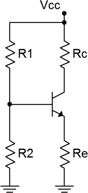
Schematic
Figure 1
Procedure
DC Load Line
Consider the circuit of Figure 1 using Vcc = 10 volts, R1 = 10 kΩ, R2 = 3.3 kΩ, Re = 4.7 kΩ and Rc = 5.6 kΩ. Using the approximation of a lightly loaded “stiff” voltage divider, determine the ideal end points of the DC load line and the Q point, and record these in Table 1.
Circuit Voltages and Beta
Continuing with the component values indicated in step one, compute the theoretical base, emitter and collector voltages, and record them in Table 2 (Theory).
Build the circuit of Figure 1 using Vcc = 10 volts, R1 = 10 kΩ, R2 = 3.3 kΩ, Re = 4.7 kΩ and Rc = 5.6 kΩ. Measure the base, emitter and collector voltages and record them in the first row of Table 2 (Experimental). Compute the deviations between theoretical and experimental and record these in the first row of Table 2 (% Deviation).
Measure the base and collector currents and record these in the first row of Table 3. Based on these, compute and record the experimental beta as well.
Swap the transistor with the second transistor and repeat steps 3 and 4 using the second rows of the tables.
Swap the transistor with the third transistor and repeat steps 3 and 4 using the third rows of the tables.
Design
The collector current of the circuit can be altered by a variety of means including changing the emitter resistance. If the base voltage is held constant, the collector current is determined by the emitter resistance via Ohm’s law. Redesign the circuit to achieve half of the quiescent collector current recorded in Table 1. Obtain a resistor close to this value, swap out the original emitter resistor and measure the resulting current. Record the appropriate values in Table 4.
Troubleshooting
Return the original emitter resistor to the circuit. Consider each of the individual faults listed in Table 5 and estimate the resulting base, emitter and collector voltages. Introduce each of the individual faults in turn and measure and record the transistor voltages in Table 5.
Computer Simulation
Build the circuit of Figure 1 in a simulator. Run a DC simulation and record the resulting transistor voltages in Table 6.
Data Tables
Table 1
VCE (Cutoff)
IC (Sat)
VCEQ
ICQ
Table 2
Transistor
VB Thry
VE Thry
VC Thry
VB Exp
VE Exp
VC Exp
%D VB
%D VE
%D VC
1
2
3
Table 3
Transistor
IB
IC
β
1
2
3
Table 4
RE Theory
RE Actual
IC Measured
Table 5
Issue
VB
VE
VC
R2 Short
RE Open
RC Short
RC Open
VCE Short
VCE Open
Table 6
VB Sim
VE Sim
VC Sim
Questions
Based on the results of Table 1, is the transistor operating in saturation, cutoff or in the linear region?
Based on the results of Tables 2 and 3, does the circuit achieve a stable operating point when compared to beta?
Based on the measurements of Table 5, is it possible for different circuit problems to produce similar or even identical voltages in the circuit, or is every fault unique in its outcome?
What is the required design condition for the voltage divider bias to achieve high Q point stability in spite of changes in beta?
Using the original circuit, determine a new value for the collector resistance that will yield a collector voltage of approximately half of the power supply value.