Want to create or adapt books like this? Learn more about how Pressbooks supports open publishing practices.
16 Common Emitter Amplifier
Learning Objective
The objective of this exercise is to examine the characteristics of a common emitter amplifier, specifically voltage gain, input impedance and output impedance. A method for experimentally determining input and output impedance is investigated along with various potential troubleshooting issues.
Theory Overview
An ideal common emitter amplifier simply multiples the input function by a constant value while also inverting the signal. The voltage amplification factor, Av, is largely a function of the AC load resistance at the collector and the internal emitter resistance, r’e. This internal resistance is, in turn, inversely proportional to the DC emitter current. Therefore, if the underlying bias is stable with changes in beta, the voltage gain will also be stable. The circuit will appear as an impedance to the signal source, Zin. This impedance is approximately equal to the base biasing resistor(s) in parallel with the impedance seen looking into the base (Zin(base)) which is approximately equal to β r’e. Consequently, the amplifier’s input impedance may experience some variation with beta. In contrast, the circuit’s output impedance as seen by the load is approximately equal to the DC collector biasing resistor.
From a practical standpoint, input and output impedance cannot be measured directly with an ohmmeter. This is because ohmmeters measure resistance by sending out a small “sensing” current. The DC bias and AC signal currents will interact with this current and produce an unreliable result. Instead, impedances can be measured indirectly through a voltage divider effect. That is, if the voltages of both legs of a voltage divider can be measured and the resistance of one of the legs is known, the remaining resistance may be determined using Ohm’s law or the voltage divider rule.
Equipment
(1) Dual adjustable DC power supply
model:
srn:
(1) DMM
model:
srn:
(1) Dual channel oscilloscope
model:
srn:
(1) Function generator
model:
srn:
(3) Small signal transistors (2N3904)
(1) 10 k Ω resistor ¼ watt
actual:
(1) 15 k Ω resistor ¼ watt
actual:
(1) 20 k Ω resistor ¼ watt
actual:
(1) 22 k Ω resistor ¼ watt
actual:
(1) 33 k Ω resistor ¼ watt
actual:
10 µF capacitors
actual:
(1) 470 µF capacitor
actual:
Schematics
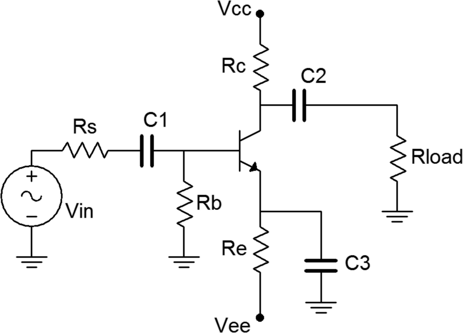
Figure 1
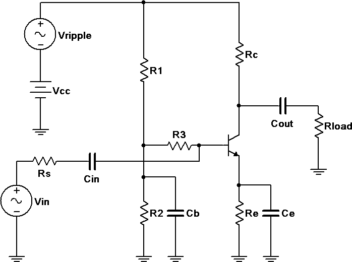
Figure 2
Procedure
DC Circuit Voltages
Consider the circuit of Figure 1 using Vcc = 15 volts, Vee = −12 volts, Rs = 10 kΩ, Rb = 33 kΩ, Re = 22 kΩ, Rc = 15 kΩ, Rload = 20 kΩ, C1 = C2 = 10 µF and C3 = 470 µF. Using the approximation of a negligible base voltage, determine the DC voltages at the base, emitter, and collector along with the collector current, and record these in Table 1.
Build the circuit of Figure 1 using Vcc = 15 volts, Vee = −12 volts, Rs = 10 kΩ, Rb = 33 kΩ, Re = 22 kΩ, Rc = 15 kΩ, Rload = 20 kΩ, C1 = C2 = 10 µF and C3 = 470 µF. Make sure that the AC source is turned off or disconnected. Measure the DC voltages at the base, emitter, and collector along with the collector current, and record these in Table 1. Note, you may wish to use a transistor curve tracer or beta checker to get approximate values of beta for each of the three transistors to be used.
AC Circuit Voltages
Based on the calculated collector current, determine the resulting theoretical r’e, Av, Zin and Zout, and record these in Table 2. Assume a beta of approximately 150 for the Zin calculation.
Continuing with the values in Table 2 and using an AC source voltage of a 40 mV peak-peak 1 kHz sine wave, compute the theoretical AC base, emitter and load voltages, and record them in Table 3 (Theory). Note that Rs will create a voltage divider effect with Zin, thus reducing the signal that reaches the base. This reduced signal is then multiplied by the voltage gain and appears at the collector.
Set the source to a 40 mV peak-peak 1 kHz sine wave and apply to the circuit. Using the oscilloscope, place one probe at the base and the second at the emitter. Record the resulting peak-peak voltages in the first row of Table 3 (Experimental). The oscilloscope inputs should be set for AC coupling with the bandwidth limit engaged. Capture an image of the oscilloscope display.
Move the second probe to the load and record its peak-peak value in the first row of Table 3. Also include whether the signal is in phase or out of phase with the base signal. Capture an image of the oscilloscope display.
Unhook the load resistor from the output capacitor and measure the resulting collector voltage (do not connect the output capacitor to ground-simply leave it dangling). Record this value in the final column of Table 3.
Reattach the load resistor. Swap the transistor with the second transistor and repeat steps 5 through 7 using the second row of Table 3.
Reattach the load resistor. Swap the transistor with the third transistor and repeat steps 5 through 7 using the third row of Table 3.
Using the measured base and collector voltages from Table 3, determine the experimental gain for each transistor. From these gains determine the experimental r’e. Using the source voltage, the measured base voltages and the source resistance, determine the effective input impedances via Ohm’s law or the voltage divider rule. Finally, in similar manner and using the loaded and unloaded collector voltages along with the load resistor value, determine the experimental output impedances. Record these values in Table 4. Also determine and record the percent deviations.
Troubleshooting
Return the load resistor to the circuit. Consider each of the individual faults listed in Table 5 and estimate the resulting AC load voltage. Introduce each of the individual faults in turn and measure and record the load voltage in Table 5.
Computer Simulation
One issue with amplifiers is noise and ripple on the power supply. This will be directly coupled to output of the circuit via the collector resistor. Worse, this noise or ripple may be coupled into the base and then amplified along with the desired input signal. This can be an issue with amplifiers that use a voltage divider bias. One way to reduce this effect is to decouple the voltage divider from the base. This modification is shown in the circuit of Figure 2. Cb effectively shorts R2, sending power supply noise and ripple to ground instead of into the base. By itself this would also short the desired input signal so an extra resistor, R3 is added between the capacitor and the base. The input impedance of the circuit is approximately equal to R3 in parallel with β r’e. To show the effectiveness of this technique, build the circuit of Figure 2 in a simulator. Use values of Vin = 20 mV peak at 1 kHz, Vripple = 20 mV peak at 120 Hz, Vcc = 12 volts, Rs = 1 kΩ, R1 = 10 kΩ, R2 = 3.3 kΩ, R3 = 22 kΩ, Re = 4.7 kΩ, Rc = 3.3 kΩ, Rload = 1 kΩ, Cin = Cout = 10 µF, Cb = 100 µF and Ce = 470 µF. Run a Transient simulation and look at the load voltage. A very small low frequency variation should be noted. This is the 120 Hz ripple coupled in through the collector resistor. Alter the circuit by removing Cb and R3 to produce the basic voltage divider circuit (or more simply, set Cb and R3 to extremely small values such as pF and mΩ). Rerun the simulation. The load voltage should now show a much more obvious ripple contribution, thus showing how effective the power supply decoupling components can be.
Data Tables
Table 1
VB Theory
VE Theory
VC Theory
IC Theory
VB Exp
VE Exp
VC Exp
IC Exp
Table 2
r’e
Av
Zin
Zout
Table 3
Transistor
VB Thry
VE Thry
VL Thry
VB Exp
VE Exp
VL Exp
Phase VL
VLNoLoad
1
2
3
Table 4
Transistor
Av Exp
r’e Exp
Zin Exp
Zout Exp
%D Av
%D r’e
%D Zin
%D Zout
1
2
3
Table 5
Issue
VLoad
RB Short
C1 Open
RC Short
RC Open
RE Open
C2 Open
C3 Open
VCE Open
Questions
Does the common emitter amplifier produce a considerable amplification effect and if so, are the results consistent across transistors?
Does the common emitter amplifier produce a phase shift at the output and if so, is it affected by the transistor beta?
If the collector and base voltages had been measured with the oscilloscope DC coupled, how would the measurements of Table 3 have changed?
Does the value of the transistor beta play any role in setting the input impedance? Was a considerable variation in input impedance apparent?