
23 Power Amp with Driver
Learning Objective
Theory Overview
Typical audio amplifiers utilize one or more small signal class A stages to achieve sufficient voltage gain which then feeds a class B power stage connected to the load (normally a loudspeaker). The stage preceding the power section is referred to as the driver stage or simply the driver. The driver is often directly coupled instead of coupled via a capacitor. This maximizes gain and reduces component count.
A typical loudspeaker exhibits a nominal 8 Ω impedance. As such, it demands considerable current. The job of the class B follower is to create a good match to this low impedance and produce sufficient current and power gain to drive it effectively. The voltage gain comes from the prior stages. If any of the amplifier stages clip the waveform, the loudspeaker will reproduce the distorted wave. This distortion can be clearly audible and produce a signal that sounds fuzzy or harsh. Loudspeakers can also be used as microphones (although the quality will not be as high as that achieved with a properly designed microphone). In this experiment, a loudspeaker will be used as a microphone to inspect the waveshapes produced by the human voice; waveshapes that are potentially far more complex than simple sine waves.
Equipment
| (1) Dual adjustable DC power supply | model: | srn: |
| (1) DMM | model: | srn: |
| (1) Dual channel oscilloscope | model: | srn: |
| (1) Function generator | model: | srn: |
| (2) Small signal NPN transistors (2N3904) | ||
| (1) Small signal PNP transistor (2N3906) | ||
| (2) Switching diodes (1N914 or 1N4148) | ||
| (2) 100 Ω resistor ¼ watt | actual: | |
| (1) 1 k Ω resistor ¼ watt | actual: | |
| (1) 6.8 k Ω resistor ¼ watt | actual: | |
| (1) 1 k Ω potentiometer or decade box | ||
| (1) 1 µF capacitor | actual: | |
| (1) 100 µF capacitor | actual: | |
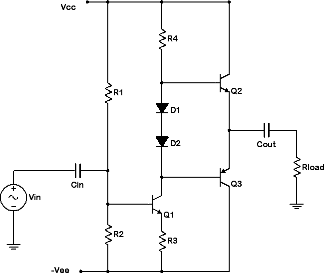
Schematic
Procedure
Bias, Gain and Compliance
- Consider the circuit of Figure 1 using Vcc = 6 volts, Vee = −6 volts, R1 = 6.8 kΩ, R4 = 1 kΩ, R3 = 100 Ω, Rload = 100 Ω, Cin = 1 µF and Cout = 100 µF. R2 is an adjustable resistance (pot or decade box). For proper bias, the emitters of the output transistors should be at 0 volts DC. For this to be true there must be a voltage of Vcc − Vbe, or approximately 5.3 volts, across R4. Ignoring base currents, this establishes the ICQ of transistor 1 which in turn creates a potential drop across R3. From this the voltage across R2 may be determined. Knowing the value of R1 and the total supply presented, Ohm’s law or the voltage divider rule may be used to compute the required setting for R2. Compute the required value for R2 and record it in Table 1.
- Compute the gain of the driver stage. For the load of Q1, the dynamic resistance of the diodes is small enough to ignore. Also, assume the current gain of the output transistors is approximately 100. Remember, only one output transistor is on at any given time. The gain of the class B stage may be assumed to be unity. Record the theoretical circuit gain in Table 1.
- Ideally, the class B stage will produce a compliance of just under 6 volts peak. It may be less than this as the driver stage might clip sooner. Compute the AC load line for the driver stage and determine its compliance. Note that there will be a voltage divider effect between Re and the load of Q1 which will reduce the compliance from that calculated via the load line. Record the theoretical compliance value in Table 1. It should be less than that of the output stage and thus represents the compliance of the entire circuit.
- Build the circuit of Figure 1 using Vcc = 6 volts, Vee = −6 volts, R1 = 6.8 kΩ, R4 = 1 kΩ, R3=100Ω, Rload = 100 Ω, Cin = 1 µF and Cout = 100 µF. Set the pot or decade box (R2) to the value calculated in Table 1. Disconnect the signal source and inspect the DC voltage at the load. Adjust R2 until this voltage goes to 0 volts. Record the resulting value of R2 in Table 1.
- Connect the signal source and apply a 1 kHz sine at 200 millivolts peak. Inspect the load and source voltages with the oscilloscope and capture an image of the pair. From these voltages determine the circuit gain and record it in Table 1.
- Increase the signal level until the output begins to clip. Reduce the level until the signal is undistorted and record the resulting load voltage as the experimental compliance in Table 1.
Waveforms: Human Perception and Production
- Turn down the signal source to about 100 mV peak. Insert the loudspeaker in series with the load resistor. Accidentally placing it in parallel will cause excessive current draw and likely destroy the output transistors (after making a particularly loud and irritating squawk). Gradually turn up the signal level while monitoring the load voltage with the oscilloscope. Listen to the sound change as the amplifier begins to clip. Describe this change in Table 2. Repeat this with the other frequencies indicated.
- Remove the loudspeaker and function generator. Reposition the loudspeaker so that it acts as the signal source (i.e., in the original position of the generator). It will now act as a microphone. While examining the load voltage, speak into the loudspeaker and note the typically complex waveshapes. Try holding a few different vowel sounds at different pitches and capture a few of these images. Ordinarily it is difficult for humans to vocalize pure sine waves, however, complex waveforms can be broken down mathematically into a combination of sine waves of differing frequencies, amplitudes and phases. As this is a linear amplifier, superposition holds, and thus if the circuit response to individual sines at differing frequencies can be determined then the response to complex waves such as the human voice and musical instruments can also be determined.
Troubleshooting
- Remove the loudspeaker and return the generator to the circuit. Consider each of the individual faults listed in Table 3 and estimate the resulting DC and AC load voltages. If the DC voltage moves a great deal off of zero, chances are the AC load voltage will be badly distorted and there is no need to attempt to estimate a precise value. Introduce each of the individual faults in turn and measure and record the load voltages in Table 3.
Data Tables
| Theory | Experimental | |
|---|---|---|
| R2 | ||
| Av | ||
| Compliance |
| Frequency | Observations |
|---|---|
|
1 kHz |
|
|
500 Hz |
|
|
200 Hz |
| Issue | VLoad DC | VLoad AC |
|---|---|---|
| R2 Short | ||
| Cin Open | ||
| R1 Open | ||
| R3 Open | ||
| D1 Short | ||
| D2 Open | ||
| Cout Open | ||
| VCE Open |
Questions
- Is the maximum output compliance determined solely by the class B output stage?
- What kinds of distortion are present in this circuit?
- Calculate the maximum load power and load current of the amplifier if the loudspeaker had accidentally been placed in parallel with the load resistor rather than in series.
- How do the values calculated in Question 3 compare to the data sheet maximums for the 2N3904/6?
