
25 JFET Amplifiers
Learning Objective
Theory Overview
In many regards, JFET amplifiers share similar attributes with their bipolar counterparts. Superficially, they look very similar as well. The main functional differences are that JFET based amplifiers tend to have higher input impedances but tend to offer lower voltage gains. Further, without swamping, JFET amplifiers tend to produce lower levels of distortion. As with r’e impacting bipolar circuit performance, JFET performance is impacted by the transconductance, gm (AKA gfs). Like the bipolar common emitter amplifier, the common source amplifier exhibits a voltage gain greater than one with inversion. The source follower, like the bipolar emitter follower, shows a voltage gain just under one with no inversion.
Equipment
| (1) Dual adjustable DC power supply | model: | srn: |
| (1) DMM | model: | srn: |
| (1) Dual channel oscilloscope | model: | srn: |
| Function generator | model: | srn: |
| (3) Small signal JFETs (MPF102, substitute J112 if not available) | ||
| (2) 4.7 k Ω resistors ¼ watt | actual: | |
| (1) 22 k Ω resistor ¼ watt | actual: | |
| (1) 33 k Ω resistor ¼ watt | actual: | |
| (1) 330 k Ω resistor ¼ watt | actual: | |
| (2) 10 µF capacitors | actual: | |
| (1) 470 µF capacitor | actual: | |
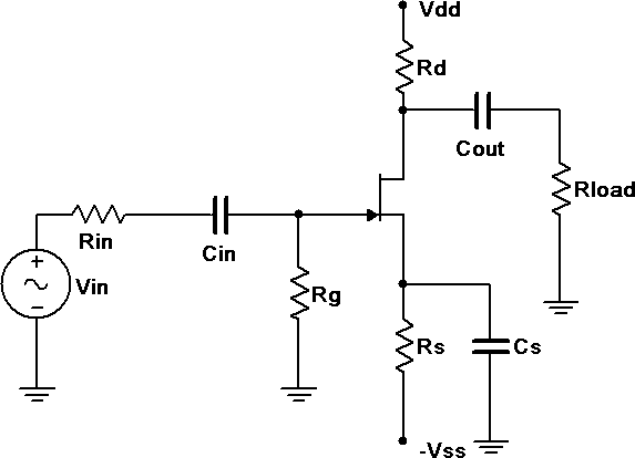
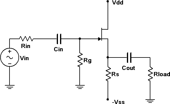
Schematics
Procedure
Common Source Voltage Amplifier
- Consider the circuit of Figure 1 using Vdd = 15 volts, Vss = −3 volts, Rin = 33 kΩ, Rg = 330 kΩ, Rs = 4.7 kΩ, Rd = 4.7 kΩ, Rload = 22 kΩ, Cin = Cout = 10 µF and Cs = 470 µF. Assuming VGS = −2 volts and gm = 2 mS (4 mS if using the J112), determine the theoretical gain and input impedance of the circuit and record these in Table 1.
- Build the circuit of Figure 1 using Vdd = 15 volts, Vss = −3 volts, Rin = 33 kΩ, Rg = 330 kΩ, Rs=4.7 kΩ, Rd = 4.7 kΩ, Rload = 22 kΩ, Cin = Cout = 10 µF and Cs = 470 µF. Set Vin to a 100 mV peak sine at 1 kHz. Measure the voltages at the gate and load, and record these in Table 1. Capture images of the input and gate voltages, and the gate and load voltages. Note whether or not the load is inverted compared to the gate signal.
- Based on the measured gate and drain voltages, determine the resulting theoretical Av and Zin, and record these in Table 1. Note that Zin may be computed using the voltage divider rule or Ohm’s law given the gate and input voltages along with the input resistor value. Also determine and record the percent deviations.
- Repeat steps 1 through 3 for the remaining two JFETs.
Common Drain Voltage Follower
- Consider the circuit of Figure 2 using Vdd = 15 volts, Vss = −3 volts, Rin = 33 kΩ, Rg = 330 kΩ, Rs = 4.7 kΩ, Rload = 22 kΩ, Cin = 10 µF and Cout = 470 µF. Assuming VGS = −2 volts and gm = 2 mS (4 mS if using the J112), determine the theoretical gain and input impedance of the circuit and record in Table 2.
- Build the circuit of Figure 2 using Vdd = 15 volts, Vss = −3 volts, Rin = 33 kΩ, Rg = 330 kΩ, Rs=4.7 kΩ, Rload = 22 kΩ, Cin = 10 µF and Cout = 470 µF. Set Vin to a 100 mV peak sine at 1 kHz. Measure the voltages at the gate and load, and record these in Table 2. Capture images of the input and gate voltages, and the gate and load voltages. Note whether or not the load is inverted compared to the gate signal.
- Based on the measured gate and drain voltages, determine the resulting theoretical Av and Zin, and record these in Table 2. Also determine and record the percent deviations.
- Repeat steps 5 through 7 for the remaining two JFETs.
Troubleshooting
- Consider each of the individual faults listed in Table 3 and estimate the resulting AC load voltage for circuit 1. Introduce each of the individual faults in turn and measure and record the load voltage in Table 3.
Data Tables
| JFET | Av Theory | Zin Theory | Vg Exp | Vd Exp | Av Exp | Zin Exp | %Dev Av | %Dev Zin |
|---|---|---|---|---|---|---|---|---|
| 1 | ||||||||
| 2 | ||||||||
| 3 |
| JFET | Av Theory | Zin Theory | Vg Exp | Vs Exp | Av Exp | Zin Exp | %Dev Av | %Dev Zin |
|---|---|---|---|---|---|---|---|---|
| 1 | ||||||||
| 2 | ||||||||
| 3 |
| Issue | VLoad |
|---|---|
| Rg Short | |
| Cin Open | |
| Rd Short | |
| Rd Open | |
| Rs Open | |
| Cout Open | |
| Cs Open | |
| VDS Open |
Exercises
- Does the common source amplifier produce a considerable amplification effect and if so, are the results consistent across transistors?
- Does the common source amplifier produce a phase shift at the load? How does this compare with the common drain follower?
- How do the voltage gains of these cir
cuits compare to their bipolar versions?
- How do the input impedances of these circuits compare to their bipolar versions?
