Want to create or adapt books like this? Learn more about how Pressbooks supports open publishing practices.
14 Feedback Biasing
Learning Objective
The objective of this exercise is to examine two kinds of feedback biasing: collector feedback and emitter feedback. Both forms potentially are more stable than simple base bias in terms of the impact of beta on collector current.
Theory Overview
By inserting a resistor in either the emitter or collector portions of the transistor circuit, it is possible to partially control the base current in such a way that an increase in beta will cause a decrease in base current which in turn helps to mitigate the tendency of collector current to increase. This will result in circuits that have greater Q point stability than simple base bias circuits although for certain practical reasons they might not be as stable as voltage divider or dual supply emitter bias schemes.
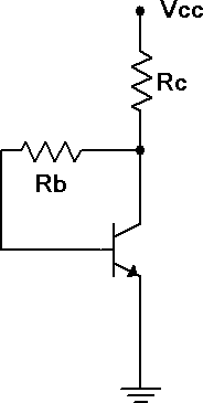
In the collector feedback arrangement, the base resistor is connected from the collector to the base. Therefore, its voltage is one base-emitter drop less than the collector voltage. The collector voltage, in turn, is simply the supply potential minus the collector resistor’s drop. Therefore, as the collector current rises, the collector resistor’s drop increases, forcing the collector voltage down and thus reducing the base resistor’s voltage. By Ohm’s law, this means that the base current must decrease. This decrease helps to limit the overall increase in collector current.
The emitter feedback situation is similar. In this instance, as collector current increases the drop across the emitter resistor rises. This will result in an increase in base voltage as it is locked to one base-emitter drop above the emitter. Consequently, as the collector current increases, the voltage across the base resistor decreases which helps to compensate for the original increase in collector current.
Equipment
(1) Adjustable DC Power Supply
model:
srn:
(1) DMM
model:
srn:
(3) Small signal transistors (2N3904)
(1) 330 Ω resistor ¼ watt
actual:
(1) 470 Ω resistor ¼ watt
actual:
(1) 1 k Ω resistor ¼ watt
actual:
(1) 220 k Ω resistor ¼ watt
actual:
Schematics
Figure 1Figure 2
Procedure
Collector Feedback – DC Load Line
Consider the circuit of Figure 1 using Vcc = 12 volts, Rb = 220 kΩ and Rc = 1 kΩ. Determine the ideal end points of the DC load line and the Q point, and record these in Table 1.
Circuit Voltages and Beta
Continuing with the component values indicated in step one, compute the theoretical base, emitter and collector voltages, and record them in Table 2 (Theory).
Build the circuit of Figure 1 using Vcc = 12 volts, Rb = 220 kΩ and Rc = 1 kΩ. Measure the base, emitter and collector voltages and record them in the first row of Table 2 (Experimental).
Measure the base and collector currents and record these in the first row of Table 3. Based on these, compute and record the experimental beta as well.
Swap the transistor with the second transistor and repeat steps 3 and 4 using the second rows of the tables.
Swap the transistor with the third transistor and repeat steps 3 and 4 using the third rows of the tables.
Stability
Based on the measurements of Table 3, determine the maximum percent change of collector current and record in Table 4. Also determine the maximum percent change of beta and record in Table 4.
Emitter Feedback – DC Load Line
Consider the circuit of Figure 2 using Vcc = 12 volts, Rb = 220 kΩ, Re = 470 Ω and Rc = 330 Ω. Determine the ideal end points of the DC load line and the Q point, and record these in Table 5.
Circuit Voltages and Beta
Continuing with the component values indicated in step one, compute the theoretical base, emitter and collector voltages, and record them in Table 6 (Theory).
Build the circuit of Figure 2 using Vcc = 12 volts, Rb = 220 kΩ, Re = 470 Ω and Rc = 330 Ω. Measure the base, emitter and collector voltages and record them in the first row of Table 6 (Experimental).
Measure the base and collector currents and record these in the first row of Table 7. Based on these, compute and record the experimental beta as well.
Swap the transistor with the second transistor and repeat steps 3 and 4 using the second rows of the tables.
Swap the transistor with the third transistor and repeat steps 3 and 4 using the third rows of the tables.
Stability
Based on the measurements of Table 7, determine the maximum percent change of collector current and record in Table 8. Also determine the maximum percent change of beta and record in Table 8.
Troubleshooting
For the emitter feedback bias circuit, consider each of the individual faults listed in Table 9 and estimate the resulting base, emitter and collector voltages. Introduce each of the individual faults in turn and measure and record the transistor voltages in Table 9.
Data Tables
Table 1
VCE (Cutoff)
IC (Sat)
VCEQ
ICQ
Table 2
Transistor
VB Theory
VE Theory
VC Theory
VB Exp
VE Exp
VC Exp
1
2
3
Table 3
Transistor
IB
IC
β
1
2
3
Table 4
% Δ β
% Δ IC
Table 5
VCE (Cutoff)
IC (Sat)
VCEQ
ICQ
Table 6
Transistor
VB Theory
VE Theory
VC Theory
VB Exp
VE Exp
VC Exp
1
2
3
Table 7
Transistor
IB
IC
β
1
2
3
Table 8
% Δ β
% Δ IC
Table 9
Issue
VB
VE
VC
RB Open
RE Open
RE Short
RC Open
RC Short
VCE Open
Questions
Based on the results of Tables 4 and 8, do these circuits achieve a stable operating point when compared to beta?
Which circuit is more stable in this exercise; the emitter feedback bias or the collector feedback bias? Is it safe to say that this will always be the case for any emitter feedback bias circuit versus any collector feedback bias circuit?
Are the transistor voltages always as stable as the collector current or can they be more or less stable?
Based on the collector current equation derivations for the two circuits, derive the collector current equation for a combination circuit which consists of a collector feedback bias circuit with an emitter resistor added.