Want to create or adapt books like this? Learn more about how Pressbooks supports open publishing practices.
17 Swamped CE Amplifier
Learning Objective
The objective of this exercise is to examine the characteristics of a swamped common emitter amplifier, specifically the effects of swamping on voltage gain, input impedance and distortion.
Theory Overview
As the signal current changes in a transistor, the total current flowing through the emitter changes along with it. As a result, these changes produce small changes in r’e which in turn changes the voltage gain. In other words, the gain changes throughout the signal producing slightly more or less gain at some points along the signal than others. These changes show up as a squashing or elongating of the positive and negative peaks of the output signal. Generally, these forms of waveform distortion are to be avoided.
Also, they tend to worsen as the output signal amplitude increases. A method of mitigating this distortion is to add AC resistance to the emitter portion of the circuit. This added resistance tends to buffer or “swamp out” the changes in r’e and therefore reduces the distortion. A side bonus is that Zin(base) will also be increased which will result in an increased Zin to the circuit. On the downside, the added resistance will lower the voltage gain. Consequently the swamped amplifier exhibits a lower gain but one of higher quality. In general, the larger the swamping resistance is compared to r’e, the greater the effects on distortion, gain and input impedance.
Equipment
(1) Dual adjustable DC power supply
model:
srn:
(1) DMM
model:
srn:
(1) Dual channel oscilloscope
model:
srn:
(1) Low distortion function generator
model:
srn:
(1) Distortion analyzer
model:
srn:
(1) Small signal transistor (2N3904)
(1) 220 Ω resistor ¼ watt
actual:
(1) 1 k Ω resistor ¼ watt
actual:
(1) 10 k Ω resistor ¼ watt
actual:
(1) 15 k Ω resistor ¼ watt
actual:
(1) 20 k Ω resistor ¼ watt
actual:
(1) 22 k Ω resistor ¼ watt
actual:
(1) 33 k Ω resistor ¼ watt
actual:
(2) 10 µF capacitors
actual:
(1) 470 µF capacitor
actual:
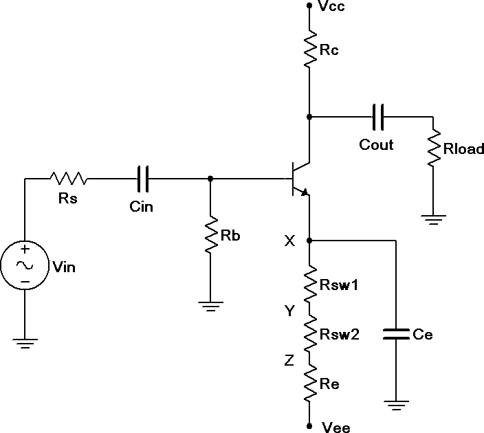
Schematic
Figure 1
Procedure
AC Circuit Voltages
Consider the circuit of Figure 1 using Vcc = 15 volts, Vee = −12 volts, Rs = 10 kΩ, Rb = 33 kΩ, Re = 22 kΩ, Rsw1 = 220 Ω, Rsw2 = 1 kΩ, Rc = 15 kΩ, Rload = 20 kΩ, Cin = Cout = 10 µF and Ce=470 µF. Using the approximation of a negligible DC base voltage, determine the DC collector current and r’e, and record these in Table 1. Using the r’e, calculate the expected Zin, Zin(base), and Av for the X, Y and Z connection points for Ce (shown at position X in the schematic). Record these in Table 2. If a transistor curve tracer or beta checker is not available to get an approximate value of beta for the transistor, estimate it at 150.
Build the circuit of Figure 1 using Vcc = 15 volts, Vee = −12 volts, Rs = 10 kΩ, Rb = 33 kΩ, Re=22 kΩ, Rsw1 = 220 Ω, Rsw2 = 1 kΩ, Rc = 15 kΩ, Rload = 20 kΩ, Cin = Cout = 10 µF and Ce=470µF. Connect Ce to postion X. Disconnect the signal source and check the DC transistor voltages to ensure that the circuit is biased correctly (note, the DC equivalent circuit is very similar to the ones used in the EmitterBias Exercise and should exhibit similar DC voltage readings).
Using a 1 kHz sine wave setting, apply the signal source to the amplifier and adjust it to achieve a load voltage of 2 volts peak-peak.
Measure the AC peak-peak voltages at the source, the base, and the load, and record these in Table 3. The load waveforms may exhibit some asymmetry due to distortion so be sure to record the peak- peak voltage not the peak. If asymmetry is observed between the positive and negative peaks, make a note of it. Also, capture images of the oscilloscope displays (Vs with Vb and Vb with Vload).
Set the distortion analyzer to 1 kHz and % total harmonic distortion (% THD). Apply it across the load and record the resulting reading in the final column of Table 3.
Remove the distortion analyzer and connect Ce to position Y instead of X. Repeat steps 3, 4 and 5.
Remove the distortion analyzer and connect Ce to point Z instead of Y. Repeat steps 3, 4 and 5.
Using the measured base and load voltages from Table 3, determine the experimental gain for the transistor. Using the measured source and base voltages along with the source resistance, determine the effective input impedances via Ohm’s law or the voltage divider rule. Record these values in Table 4. Also determine and record the percent deviations.
Computer Simulation
Build the circuit in a simulator and run three sets of simulations, one for each of the three Ce positions. For each trial, set the AC source voltage to the value measured in Table 3 (VS Exp). Run a Transient Analysis and inspect the voltages at the base and load. The AC source voltage may have to be adjusted slightly to achieve the desired the desired 2 volt peak-peak load voltage. Record these values in Table 5. Run the Distortion or Fourier Analysis at the load and record the resulting THD value in Table 5 as well.
Data Tables
Table 1
IC
r’e
Table 2
Position
Av Theory
Zin(Base) Theory
Zin Theory
X
Y
Z
Table 3
Position
VS Exp
VB Exp
VL Exp
% THD
X
Y
Z
Table 4
Position
Av Exp
Zin Exp
%Dev Av
%Dev Zin
X
Y
Z
Table 5
Position
VS Sim
VB Sim
VL Sim
% Distortion
X
Y
Z
Questions
In summary, what are the effects of swamping?
Is the change in voltage gain directly proportional to the amount of swamping?
Is the change in input impedance directly proportional to the amount of swamping?
Is the change in distortion directly proportional to the amount of swamping?
Are THD levels below 1% easily discerned on a simple oscilloscope display?
Why is it important that the load voltage be set to the same value in each of the three trials instead of setting the source to the same value?