Want to create or adapt books like this? Learn more about how Pressbooks supports open publishing practices.
18 Emitter Bias
Learning Objective
The objective of this exercise is to examine the two supply emitter bias topology and determine whether or not it produces a stable Q point. Various potential troubleshooting issues are also explored.
Theory Overview
One of the problems with simpler biasing schemes such as the base bias is that the Q point (IC and VCE) will fluctuate with changes in beta. This will result in inconsistent circuit performance. If a fixed voltage can be developed across an emitter resistor, a stable Q point will result. To obtain this fixed emitter resistor voltage, a negative voltage supply may be connected to the low side of the emitter resistor instead of connecting that resistor to ground. The transistor’s base is then simply connected back to ground via a single resistor. If this base resistance is relatively small, the base voltage will be close to zero as only the base current flows through it. Consequently, almost all of the negative emitter supply will drop across the emitter resistor, with the exception of the single base-emitter potential. This will result in a stable emitter current, and by extension, stable collector current and collector-emitter voltage. As beta varies, this change will be reflected in a change in base current. This can result in large percentage changes in base voltage; however, the magnitude of the base potential will remain small, and thus, inconsequential.
Equipment
(1) Dual adjustable DC power supply
model:
srn:
(1) DMM
model:
srn:
(3) Small signal transistors (2N3904)
(1) 15 k Ω resistor ¼ watt
actual:
(1) 22 k Ω resistor ¼ watt
actual:
(1) 33 k Ω resistor ¼ watt
actual:
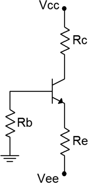
Schematic
Figure 1
Procedure
DC Load Line
Consider the circuit of Figure 1 using Vcc = 15 volts, Vee = −12 volts, Rb = 33 kΩ, Re = 22 kΩ and Rc = 15 kΩ. Using the approximation of a negligible base voltage, determine the ideal end points of the DC load line and the Q point, and record these in Table 1.
Circuit Voltages and Beta
Continuing with the component values indicated in step one, compute the theoretical emitter and collector voltages, and record them in Table 2 (Theory). For the theoretical base voltage entry, assume a beta of approximately 150 and determine the base current and voltage from the theoretical collector current recorded in the Table 1.
Build the circuit of Figure 1 using Vcc = 15 volts, Vee = −12 volts, Rb = 33 kΩ, Re = 22 kΩ and Rc = 15 kΩ. Measure the base, emitter and collector voltages and record them in the first row of Table 2 (Experimental). Compute the deviations between theoretical and experimental and record these in the first row of Table 2 (% Deviation).
Measure the base and collector currents and record these in the first row of Table 3. Based on these, compute and record the experimental beta as well.
Swap the transistor with the second transistor and repeat steps 3 and 4 using the second rows of the tables.
Swap the transistor with the third transistor and repeat steps 3 and 4 using the third rows of the tables.
Design
The collector voltage of the circuit can be altered by a variety of means including changing the collector resistance. If the emitter supply and resistance are held constant, the collector voltage is determined by the collector resistance and the collector supply. Redesign the circuit to achieve a collector voltage of approximately 10 volts. Obtain a resistor close to this value, swap out the original collector resistor and measure the resulting voltage. Record the appropriate values in Table 4.
Troubleshooting
Return the original collector resistor to the circuit. Consider each of the individual faults listed in Table 5 and estimate the resulting base, emitter and collector voltages. Introduce each of the individual faults in turn and measure and record the transistor voltages in Table 5.
Computer Simulation
Build the circuit of Figure 1 in a simulator. Run a DC simulation and record the resulting transistor voltages in Table 6.
Data Tables
Table 1
VCE (Cutoff)
IC (Sat)
VCEQ
ICQ
Table 2
Transistor
VB Theory
VE Theory
VC Theory
VB Exp
VE Exp
VC Exp
%D VB
%D VE
%D VC
1
2
3
Table 3
Transistor
IB
IC
β
1
2
3
Table 4
RC Theory
RC Actual
VC Measured
Table 5
Issue
VB
VE
VC
RB Short
RB Open
RC Short
RC Open
RE Open
VCE Open
Table 6
VB Sim
VE Sim
VC Sim
Questions
Based on the results of Table 1, is the transistor operating in saturation, cutoff or in the linear region?
Based on the results of Tables 2 and 3, does the circuit achieve a stable operating point when compared to beta?
How does the Emitter Bias circuit compare to Base Bias in terms of Q point stability and complexity?
Using the original circuit, determine a new value for the emitter resistance that will yield half of the quiescent collector current recorded in Table 1.