Want to create or adapt books like this? Learn more about how Pressbooks supports open publishing practices.
19 Frequency Limits
Learning Objective
This exercise focuses on the analysis of the frequency limits of a transistor amplifier. The elements contributing to both the lower and upper limits of frequency performance are examined, thus defining the midband region of the circuit.
Theory Overview
As the signal frequency extends to very high or very low frequencies, capacitive effects on gain can no longer be ignored or idealized as shorts or opens. At low frequencies, coupling and bypass capacitors in conjunction with surrounding resistance create lead networks that cause a reduction in voltage gain. At higher frequencies, small shunting capacitances associated with individual devices and circuit wiring create lag networks. These will also create a reduction in voltage gain. In general, the highest critical frequency among the lead networks creates the amplifier’s lower limit frequency, f1. In contrast, the lowest critical frequency among the lag networks creates the amplifier’s upper limit frequency, f2. These points are defined as the half-power points and can be determined experimentally by finding those frequencies at which the output voltage (and hence, voltage gain) has fallen to 70.7% of the midband value. The values are found theoretically by Thevenizing the circuitry around the capacitor in question, reducing it to a single resistance, and solving for the critical frequency, fc.
Equipment
(1) Dual adjustable DC power supply
model:
srn:
(1) DMM
model:
srn:
(1) Dual channel oscilloscope
model:
srn:
(1) Function generator
model:
srn:
(1) Small signal transistor (2N3904)
(1) 10 k Ω resistor ¼ watt
actual:
(1) 15 k Ω resistor ¼ watt
actual:
(1) 20 k Ω resistor ¼ watt
actual:
(1) 33 k Ω resistor ¼ watt(1) 15 k Ω resistor ¼ watt
actual:
(1) 2.2 nF capacitor
actual:
(1) 10 nF capacitor
actual:
(2) 10 µF capacitors
actual:
(1) 470 µF capacitor
actual:
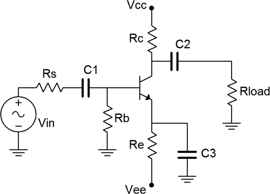
Schematic
Figure 1
Procedure
Midband Response
The circuit of Figure 1 is the same as the one used in the Common Emitter Amplifier exercise. The values used were Vcc = 15 volts, Vee = −12 volts, Rs = 10 kΩ, Rb = 33 kΩ, Re = 22 kΩ,Rc= 15 kΩ, Rload = 20 kΩ, C1 = C2 = 10 µF and C3 = 470 µF. It was shown that the amplifier produced considerable voltage at 1 kHz. Build the circuit using these values and verify that it is operating correctly by setting Vin to a 40 mV peak-peak sine wave at 1 kHz and measuring Vout. Compute the voltage gain and record these two values in Table 1.
Compute the expected critical frequencies of the input and output coupling networks along with the emitter bypass network and record the values in Table 2. Include the Thevenized resistance for each equivalent circuit.
Lower Frequency Limit
The input coupling network can be made clearly dominant by replacing C1 with a smaller value. Decreasing C1 from 10 µF to 10 nF will increase its critical frequency by a factor of 1000. Replace C1 with this value.
Set the AC source voltage to a 40 mV peak-peak 10 kHz sine wave. Note the output level at the load. Sweep the frequency between 5 kHz and 20 kHz to verify that the gain is stable. Decrease the input frequency until the load signal drops to 70.7% of the 10 kHz level. Record this value in Table 3.
The output network may be examined in a similar fashion. Return C1 to 10 µF, replace C2 with a10 nF and repeat step 4.
Return C2 to the original 10 µF capacitor before proceeding.
Upper Frequency Limit
The upper frequency limit is controlled by small device and wiring capacitances that will vary with the precise components used and the circuit layout. To minimize potential errors, a large load capacitance can be shunted across Rload to bring the critical frequency down to an easily managed frequency. This could also represent the effect of cable capacitance.
Place a 2.2 nF capacitor across the load. Compute the effective resistance of the lag network and its corresponding critical frequency in Table 4.
Set the AC source voltage to a 40 mV peak-peak 1 kHz sine wave. Note the output level at the load. Sweep the frequency around 1 kHz to verify that the gain is stable. Increase the input frequency until the load signal drops to 70.7% of the 1 kHz level. Record this value in Table 4.
Computer Simulation
Perform an AC Analysis (Bode plot) of the amplifier using the original capacitor values and for the three variations. Plot the gain from 1 Hz to 10 MHz for the original circuit and from 10 Hz to 100 kHz for the three variations. Compare the simulated results to the experimental values.
Data Tables
Table 1
Vin
Vout
Av
Table 2
Network
Rthev
fc
Input
Output
Bypass
Table 3
Capacitor
fc Theory
fc Exp
%Dev
C1=10 nF
C2=10 nF
Table 4
Rout
fout Theory
fout Exp
%Dev
Questions
What effect might resistor and capacitor tolerance have on critical frequencies?
Does beta variation have an impact on frequency response? If so, how?
Explain the possible effects of load impedance on the frequency response of the amplifier.