Want to create or adapt books like this? Learn more about how Pressbooks supports open publishing practices.
20 Voltage Follower
Learning Objective
The objective of this exercise is to examine the characteristics of a voltage follower, specifically an emitter follower using a Darlington pair. Voltage gain, input impedance and distortion will all be examined.
Theory Overview
The function of a voltage follower is to present a high input impedance and a low output impedance with a non-inverting gain of one. This allows the load voltage to accurately track or follow the source voltage in spite of a large source/load impedance mismatch. Ordinarily this mismatch would result in a large voltage divider loss. Consequently, followers are often used to drive a low impedance load or to match a high impedance source. While typical laboratory sources exhibit low internal impedances, some circuits and passive transducers can exhibit quite high internal impedances. For example, electric guitar pickups can exhibit in excess of 10 k Ω at certain frequencies. Although the voltage gain may be approximately one, current gain and power gain can be quite high, especially if a Darlington pair is used. Besides unity voltage gain and a high Zin and low Zout, followers also tend to exhibit low levels of distortion.
The Darlington pair effectively produces a “beta times beta” effect by feeding the emitter current of one device into the base of a second transistor. This also produces the effect of doubling both the effective VBE and r’e.
Equipment
(1) Dual adjustable DC power supply
model:
srn:
(1) DMM
model:
srn:
(1) Dual channel oscilloscope
model:
srn:
(1) Low distortion function generator
model:
srn:
(1) Distortion analyzer
model:
srn:
(2) Small signal transistors (2N3904)
(1) 220 Ω resistor ¼ watt
actual:
(1) 1 k Ω resistor ¼ watt
actual:
(1) 22 k Ω resistor ¼ watt
actual:
(1) 470 k Ω resistor ¼ watt
actual:
(1) 10 µF capacitor
actual:
(1) 470 µF capacitor
actual:
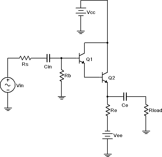
Schematic
Figure 1
Procedure
Consider the circuit of Figure 1 using Vcc = 5 volts, Vee = −12 volts, Rs = 22 kΩ, Rb = 470 kΩ, Re = 1 kΩ, Rload = 220 Ω, Cin = 10 µF and Ce = 470 µF. Using the approximation of a negligible DC base voltage, determine the DC collector current and r’e, and record these in Table 1. Using the r’e, calculate the expected Zin, Zin(base), Zout and Av. Record these in Table 2. If a transistor curve tracer or beta checker is not available to get an approximate value of beta for the transistors, estimate the pair at 10,000.
Build the circuit of Figure 1 using Vcc = 5 volts, Vee = −12 volts, Rs = 22 kΩ, Rb = 470 kΩ, Re=1kΩ, Rload = 220 Ω, Cin = 10 µF and Ce = 470 µF. Disconnect the signal source and check the DC transistor voltages to ensure that the circuit is biased correctly. (Note: The base should be close to zero while the emitter will be two VBE drops less, or about −1.4 VDC.)
Using a 1 kHz sine wave setting, apply the signal source to the amplifier and adjust it to achieve a source voltage of 2 volts peak-peak (i.e., to the left of Rs).
Measure the AC peak-peak voltages at the source, the base, and the load, and record these in Table 3. Also note the phase of the load voltage compared to the source. If distortion asymmetry is observed between the positive and negative peaks, make a note of it. Also, capture images of the oscilloscope displays (Vs with Vb and Vb with Vload).
Set the distortion analyzer to 1 kHz and % total harmonic distortion (% THD). Apply it across the load and record the resulting reading in Table 3.
Finally, unhook (i.e., open) the load and measure the resulting load voltage. Record this in the final column of Table 3.
Using the measured base and load voltages from Table 3, determine the experimental gain for the circuit. Using the measured source and base voltages along with the source resistance, determine the effective input impedance via Ohm’s law or the voltage divider rule. In similar fashion, using the loaded and unloaded load voltages along with the load resistance, determine the effective output impedance. Record these values in Table 4. Also determine and record the percent deviations.
Troubleshooting
Return the load resistor to the circuit. Consider each of the individual faults listed in Table 5 and estimate the resulting AC load voltage. Introduce each of the individual faults in turn and measure and record the load voltage in Table 5.
Computer Simulation
Build the circuit in a simulator and run a Transient Analysis. Use a 1 kHz 1 volt peak sine for the source. Inspect the voltages at the source, base and load. Record these values in Table 6. Run the Distortion or Fourier Analysis at the load and record the resulting THD value in Table 6.
Data Tables
Table 1
IC
r’e
Table 2
Av Theory
Zin(Base) Theory
Zin Theory
Zout Theory
Table 3
VS Exp
VB Exp
VL Exp
Phase VL
% THD
VLNoLoad
Table 4
Av Exp
Zin Exp
Zout Exp
%Dev Av
%Dev Zin
%Dev Zout
Table 5
Issue
VLoad
Rb Short
Cin Open
Re Open
Ce Open
RLoad Short
VCE Open
VCC Open
Table 6
VS Sim
VB Sim
VL Sim
% Distortion
Questions
Would the results of this exercise have been considerably different if the load had been ten times larger? What does that say about the performance of the circuit?
If the 22 k source had been directly connected to the 220 load without the follower in between, what would be the load voltage?
How do the THD levels of the follower compare to those of the swamped common emitter amplifier?
How would the circuit parameters change if a Darlington pair had not been used?