Want to create or adapt books like this? Learn more about how Pressbooks supports open publishing practices.
22 Class B Power Analysis
Learning Objective
The objective of this exercise is to examine large signal class B operation. A voltage follower will be investigated to determine output compliance, maximum load power, supplied DC power and efficiency. The effects of crossover distortion will be noted by comparing resistor and diode biasing schemes.
Theory Overview
The maximum output signal, or compliance, of a class B amplifier is determined by its AC load line. The peak to peak compliance is roughly equal to the total DC supply voltage(s). As two output devices are used, each conducting for half of the cycle, the quiescent current can remain low, unlike a class A amplifier. This results in vastly improved efficiency, theoretically up to 78.5%. The switchover from one transistor to the other is problematic and can result in crossover or notch distortion. To alleviate this, the transistors are given a small idle current so that each base-emitter junction is just about fully on. While resistors can be used to create this bias, trying to match the linear current-voltage characteristic of a resistor to the logarithmic characteristic of a PN junction is tricky. Consequently, another PN junction, namely a diode, is used instead. The diode will result in a more stable circuit which produces less notch distortion.
Equipment
(1) Dual adjustable DC power supply
model:
srn:
(1) DMM
model:
srn:
(1) Dual channel oscilloscope
model:
srn:
(1) Low distortion function generator
model:
srn:
(1) Distortion analyzer
model:
srn:
(1) Small signal NPN transistor (2N3904)
(1) Small signal PNP transistor (2N3906)
(2) Switching diodes (1N914 or 1N4148)
(1) 100 Ω resistor ¼ watt
actual:
(2) 220 Ω resistor ¼ watt
actual:
(2) 2.2 k Ω resistor ¼ watt
actual:
(2) 10 µF capacitor
actual:
(1) 100 µF capacitor
actual:
Schematics
Figure 1
Figure 2
Figure 3
Procedure
Resistor versus Diode Bias and Crossover Distortion
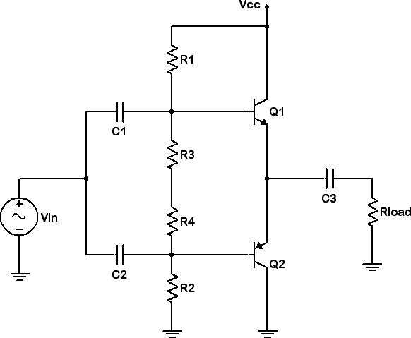
Consider the circuit of Figure 1 using Vcc = 6 volts, R1 = R2 = 2.2 kΩ, R3 = R4 = 220 Ω, Rload = 100 Ω, C1 = C2 = 10 µF and C3 = 100 µF. Ideally this circuit will produce a compliance of just under 6 volts peak-peak.
Build the circuit of Figure 1 using Vcc = 6 volts, R1 = R2 = 2.2 kΩ, R3 = R4 = 220 Ω, Rload = 100Ω, C1 = C2 = 10 µF and C3 = 100 µF. Disconnect the signal source and insert an ammeter into the collector of Q1. Record ICQ in Table 1.
Connect the signal source and apply a 1 kHz sine at 2 volts peak. Look at the load voltage and capture the oscilloscope image. There should be considerable notch or crossover distortion.
Cycle through the remaining supply voltages in Table 1, repeating steps 2 and 3. Only images of the first and last trials need be captured. As the bias current increases, the notch distortion should decrease.
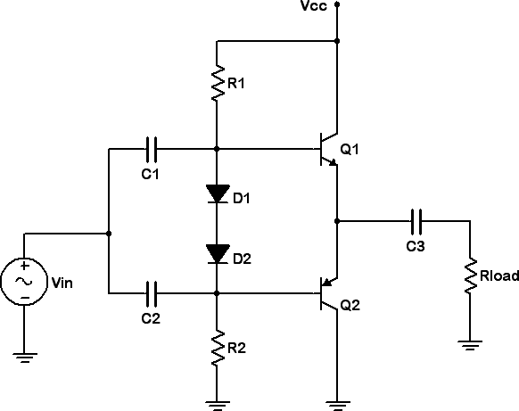
Replace R3 and R4 with switching diodes, as shown in Figure 2. Repeat steps 2 through 4 using this circuit and Table 2. Overall, the superior matching of the diodes to the transistors should result in decreased notch distortion.
Dual Supply and Power Analysis
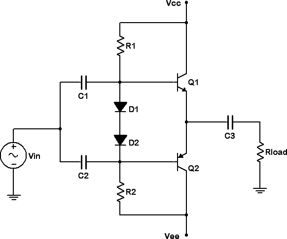
Add the negative power supply so that the circuit now appears as Figure 3. Set the power supplies to +/−6 volts DC. This should produce similar bias and amplification results to the single 12 volt supply circuit of Figure 2. Although the output coupling capacitor is no longer needed (one advantage of the dual supply topology), leave it in for safety sake.
Based on the ICQ recorded for the 12 volt supply in Table 2, determine the theoretical PDQ. Also determine the expected compliance, PLoad(max), Isupplied, Psupplied and efficiency. Record these values in the Theoretical column of Table 3.
Apply the signal source to the amplifier and adjust it to achieve a load voltage that just begins to clip. Reduce the amplitude slightly to produce a clean, unclipped wave. Record this level as the experimental compliance in Table 3. From this, determine and record the experimental maximum load power. Also, capture an image of the oscilloscope display.
Insert an ammeter in the collector and measure the resulting current with the signal still set for maximum unclipped output. Record this in Table 3 as I supplied (Experimental). Remove the ammeter.
Using the data already recorded, determine and record the experimental PDQ, PSupplied, and η. Finally, determine the deviations for Table 3.
Distortion
Unlike class A distortion which gets worse as the signal increases, notch distortion is relatively fixed. Therefore, it represents a smaller percentage of the overall output signal as the signal increases. To see this effect, adjust the signal level to achieve a load voltage of 8 volts peak-peak. There should be no clipping. Set the distortion analyzer to 1 kHz and % total harmonic distortion (% THD). Apply it across the load and record the resulting reading in Table 4 (8 Vpp). Decrease the generator to achieve a load voltage of 1 volt peak-peak and record the resulting THD.
Computer Simulation
Build the circuit in a simulator and run a Transient Analysis. Use a 1 kHz 7 volt peak sine for the source. Inspect the voltage at the load. Record the peak clip points in Table 5. Reduce the input signal so that clipping disappears. Run the Distortion or Fourier Analysis at the load and record the resulting THD value in Table 5.
Data Tables
Table 1
Supply
ICQ – Resistors
6 V
8 V
10 V
12 V
Table 2
Supply
ICQ – Diodes
6 V
8 V
10 V
12 V
Table 3
Theory
Experimental
% Deviation
Compliance
PLoad(max)
ISupplied
PDQ
PSupplied
η
Table 4
%THD 8 Vpp
%THD 1 Vpp
Table 5
Positive Clip
Negative Clip
% Distortion
Questions
Does the maximum load power compare favorably to the supplied DC power and the transistor’s power dissipation? That is, is the circuit efficient? How does it compare to class A operation (Exercise 12)?
How is the notch distortion affected by the power supply?
Compare the resistor bias and diode bias circuits regarding idle current (ICQ) and notch distortion. Compute the ICQ versus VCC stability (ICQ-MAX / ICQ-MIN) of each circuit using the first and last entries of Tables 1 and 2.
How does the class B circuit distortion compare to class A operation (Exercise 12)?
Would increasing the Vcc supply increase the output compliance? Why/why not?