
15 PNP Transistors
Learning Objective
Theory Overview
On a practical level, PNP transistors may be thought of as a mirror image of their NPN counterparts. That is, all of the device’s voltage polarities and current directions will be opposite of those found with NPNs. In fact, a simple way to turn an NPN circuit into an equivalent PNP circuit is to swap out the transistor and then flip the polarity of the power supply (or supplies, as the case may be). The resulting circuit will produce essentially the same voltages and currents as the original but with reversed polarities. By no means are negative power supplies a requirement to use PNPs, though. Commonly, the circuit is “flipped top to bottom” and implemented with a positive supply. In this case the emitter will be found toward the top and the collector toward the bottom. In some instances this orientation may also reverse the operational logic of the circuit. For example, the “flipped” PNP LED driver becomes an inverting driver. That is, a logic low will light the LED instead of a logic high.
Equipment
| (1) Adjustable DC Power Supply | model: | srn: |
| (1) DMM | model: | srn: |
| (3) Small signal PNP transistors (2N3906) | ||
| (1) LED | ||
| (1) 220 Ω resistor ¼ watt | actual: | |
| (1) 3.3 k Ω resistor ¼ watt | actual: | |
| (1) 4.7 k Ω resistor ¼ watt | actual: | |
| (1) 5.6 k Ω resistor ¼ watt | actual: | |
| (1) 10 k Ω resistor ¼ watt | actual: | |
Link
Download the datasheet:
Schematics
Procedure
PNP Voltage Divider
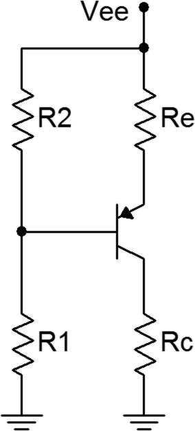
- Consider the circuit of Figure 1 using Vee = 10 volts, R1 = 10 kΩ, R2 = 3.3 kΩ, Re = 4.7 kΩ and Rc = 5.6 kΩ. Using the approximation of a lightly loaded “stiff” voltage divider, determine the theoretical base, emitter and collector voltages, and record them in Table 1 (Theory).
- Build the circuit of Figure 1 using Vee = 10 volts, R1 = 10 kΩ, R2 = 3.3 kΩ, Re = 4.7 kΩ and Rc= 5.6 kΩ. Measure the base, emitter and collector voltages and record them in the first row of Table 1 (Experimental).
- Swap the transistor with the second transistor and repeat steps 1 and 2 using the second row of the table.
- Swap the transistor with the third transistor and repeat steps 1 and 2 using the third row of the table.
Troubleshooting
- Consider each of the individual faults listed in Table 2 and estimate the resulting base, emitter and collector voltages. Introduce each of the individual faults in turn and measure and record the transistor voltages in Table 2.
PNP LED Driver
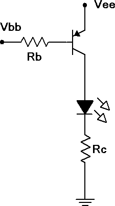
- Consider the PNP saturating switch of Figure 2 using Vee = Vbb = 5 volts, Rb = 4.7 kΩ and Rc = 220 Ω. Calculate the base and collector currents and record them in the first row of Table 3 (Theory). As the circuit is in saturation, the theoretical VCE is close to zero and may be found on the transistor data sheet via the VCE/IC saturation graph. Record this value in the first row of Table 3 as well.
- Build the saturating switch of Figure 2 using Vee = Vbb = 5 volts, Rb = 4.7 kΩ and Rc = 220 Ω. Measure and record the base and collector currents, and record the collector-emitter voltage in the first row of Table 3 (Experimental). Also compute and record the deviations between theory and experimental results.
- Remove the base resistor from Vbb and connect it to ground. Without a base source potential, the circuit will be in cutoff. Determine the theoretical base and collector currents along with the collector- emitter voltage and record them in the second row of Table 3. Measure these parameters, record them in Table 3, and also compute and record the resulting deviations.
- Reconnect the base resistor to the Vbb supply and swap in the second transistor. Repeat steps 3 and 4 using the next two rows of Table 3.
- Reconnect the base resistor to the Vbb supply and swap in the third transistor. Repeat steps 3 and 4 using the final two rows of Table 3.
Design
- A simple way to program the LED current in the driver is by altering the collector resistor. First, measure the LED potential while it is lit. Assuming that the collector-emitter saturation voltage is negligible, all of the power supply voltage will drop across the collector resistor when the LED is lit, with the exception of the LED voltage. Ohm’s law can then be used to determine a resistance value for a desired target current. Compute the required value of resistance to achieve an LED current of 8 mA. Replace the collector resistor with the nearest value available and measure the resulting current. Record the appropriate values in Table 4.
Data Tables
| Transistor | VB Thry | VE Thry | VC Thry | VB Exp | VE Exp | VC Exp |
|---|---|---|---|---|---|---|
| 1 | ||||||
| 2 | ||||||
| 3 |
| Issue | VB | VE | VC |
|---|---|---|---|
| R2 Short | |||
| RE Open | |||
| RC Short | |||
| RC Open | |||
| VCE Short | |||
| VCE Open |
| Vbb | IB Theory | IC Theory | VCE Theory | IB Exp | IC Exp | VCE Exp |
|---|---|---|---|---|---|---|
| 5 | ||||||
| 0 | ||||||
| 5 | ||||||
| 0 | ||||||
| 5 | ||||||
| 0 |
| RC Theory | RC Actual | IC Measured |
|---|---|---|
Questions
- Is the PNP voltage divider circuit as stable as its NPN counterpart studied earlier?
- Compare the NPN voltage divider lab results to this PNP version. If the various transistor voltages are added together (e.g., NPN base voltage plus PNP base voltage), a constant results. What is the significance of this value and will it always work out in this fashion? Why/why not?
- Do the troubleshooting faults presented in the PNP circuit produce similar transistor voltages compared to the same faults in the NPN version of the circuit? Why/why not?
- How does the operational logic of the PNP LED driver compare to the NPN version of the same circuit?
- Are the LED current design considerations the same as those of the NPN version?
