14.3 Differentiators
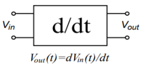
Differentiators perform the complementary function to the integrator. The base form of the differentiator is shown in Figure 10.3.1 . The output voltage is the differential of the input voltage. This is very useful for finding the rate at which a signal varies over time. For example, it is possible to find velocity given distance and acceleration given velocity. This can be very useful in process control work.
Essentially, the differentiator tends to reinforce fast signal transitions. If the input waveform is non-changing, (i.e., DC), the slope is zero, and thus the output of the differentiator is zero. On the other hand, an abrupt signal change such as the rising edge of a square wave produces a very large slope, and thus the output of the differentiator will be large. In order to create the differentiation, an appropriate device needs to be associated with the op amp circuit. This was the approach taken with the integrator, and it remains valid here. In fact, we are left with the same two options: using either an inductor, or a capacitor. Again, capacitors tend to be somewhat easier to work with than inductors and are preferred. The only difference between the integrator and the differentiator is the position of the capacitor. Instead of placing it in the 𝑅𝑓 position, the capacitor will be placed in the 𝑅𝑖 position. The resulting circuit is shown in Figure 10.3.2 .

The analysis starts with the basic capacitor Equation (Equation 10.2.1):
![]()
We already know from previous work that the output voltage appears across 𝑅𝑓 , though inverted.
![]()
Also, by Ohm’s law,
![]()
By using the approximation that all input current flows through 𝑅𝑓 (since the op amp’s input current is zero), and then substituting Equation 10.2.1 for the current, we find
![]()
A quick inspection of the circuit shows that all of the input voltage drops across the capacitor, because the op amp’s inverting input is a virtual ground. Bearing this in mind, we arrive at the final output voltage equation,
![]()
(10.3.1)
As with the integrator, a leading constant is added to the fundamental form. Again, it is possible to scale the output as required through the use of gain or attenuation networks.
Accuracy and Usefulness of Differentiation
Equation 10.3.1 is an accurate reflection of the circuit response so long as the base assumptions remain valid. As with the integrator, practical considerations tend to force limits on the circuit’s operating range. If the circuit is analyzed at discrete points in the frequency domain, it can be modeled as an inverting amplifier with the following gain equation:
![]()
Note that as the frequency decreases, X_C grows, thus reducing the gain. Conversely, as the input frequency is raised, X_C falls in value, causing the gain to rise. This rise will continue until it intersects the open-loop response of the op amp. The resulting amplitude response is shown in Figure 10.3.3 .
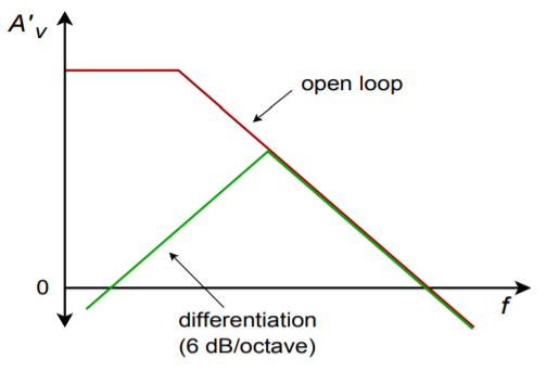
This response is the mirror image of the basic integrator response and exhibits a slope of 6 dB per octave. Note that DC gain is zero, and therefore the problems created by input bias and offset currents are not nearly as troublesome as in the integrator. Because of this, there is no limit as to how low the input frequency may be, excluding the effects of signal-to-noise ratio. Things are considerably different on the high end though. Once the circuit response breaks away from the ideal 6 dB per octave slope, differentiation no longer takes place.
Optimizing the Differentiator
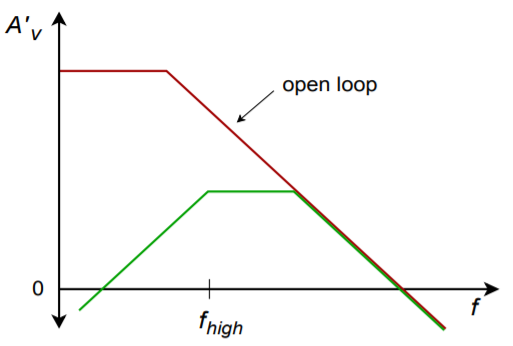
There are a couple of problems with the general differentiator of Figure 10.3.2 . First of all, it is quite possible that the circuit may become unstable at higher frequencies. Also, the basic shape of the amplitude response suggests that high frequencies are accentuated, thus increasing the relative noise level. Both of these problems may be reduced by providing an artificial upper-limit frequency, 𝑓ℎ𝑖𝑔ℎ . This tailoring may be achieved by shunting 𝑅𝑓 with a small capacitor. This reduces the high frequency gain, and thus reduces the noise. The resulting response is shown in Figure 10.3.4 .
We find 𝑓ℎ𝑖𝑔ℎ in the standard manner:
![]()
(10.3.2)
𝑓ℎ𝑖𝑔ℎ represents the highest frequency for differentiation. It is the 50% accuracy point. For higher accuracy, the input frequency must be kept well below 𝑓ℎ𝑖𝑔ℎ . At about 0.1 𝑓ℎ𝑖𝑔ℎ , the accuracy of Equation 10.3.1 is about 99%. Generally, you have to be somewhat more conservative in the estimation of accuracy than with the integrator. This is because complex waves contain harmonics that are higher than the fundamental. Even though the fundamental may be well within the high accuracy range, the upper harmonics may not be.
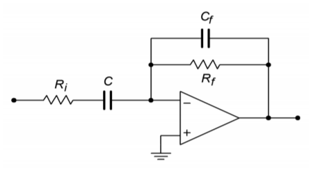
The other major problem of the basic circuit is that the input impedance is inversely proportional to the input frequency. This is because 𝑋𝐶 is the sole input impedance factor. This may present a problem at higher frequencies because the impedance will approach zero. To circumvent this problem, a resistor may be placed in series with the input capacitor in order to establish a minimum impedance value. Unfortunately, this will also create an upper break frequency, 𝑓ℎ𝑖𝑔ℎ .
![]()
(10.3.3)
The resulting response is shown in Figure 10.3.5 . The effective 𝑓ℎ𝑖𝑔ℎ for the system will be the lower of Equations 10.3.2 and 10.3.3 .

The completed, practical differentiator is shown in Figure 10.3.8 . Note that a bias compensation resistor may be required at the noninverting input, although it is not shown.
Analyzing Differentiators with the Time-Continuous Method
The time-continuous method will be used when the input signal may be easily written in the time-domain (e.g., sine waves). For more complex waveforms, such as a triangle wave, a discrete time method will be used. The continuous method will lead directly to a time-domain representation of the output waveform. Specific voltage/time coordinates will not be evaluated.
Example 10.3.1
Determine the useful range for differentiation in the circuit of Figure 10.3.9 . Also determine the output voltage if the input signal is a 2 V peak sine wave at 3 kHz.
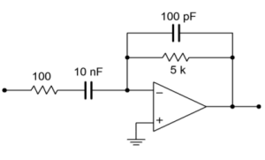
The upper limit of the useful frequency range will be determined by the lower of the two 𝑅𝐶 networks.
![]()
[f_{high (fdbk)} = \frac{1}{2 \pi \times 5 k \times 100 pF} \]
[f_{high (fdbk)} = 318.3 kHz \\ f_{high (in)} = \frac{1}{2 \pi R_f C} \]
[f_{high (in)} = \frac{1}{2 \pi \times 100 \times 10 nF} \]
[f_{high (in)} = 159.2 kHz \]
Therefore, the upper limit is 159.2 kHz. Remember, the accuracy at this limit is relatively low, and normal operation will typically be several octaves lower than this limit. Note that the input frequency is 3 kHz, so high accuracy should result. First, write 𝑉𝑖𝑛as a time-domain expression:
![]()
[V_{out}(t) = −R_f C \frac{dV_{in} (t)}{dt} \]
[V_{out}(t) = -5 k \times 10 nF \frac{d 2 \sin 2 \pi 3000t}{dt} \]
[V_{out}(t) = -10^{−4} \frac{d \sin 2 \pi 3000t}{dt} \]
[V_{out}(t) = -1.885 \cos 2 \pi 3000t \]
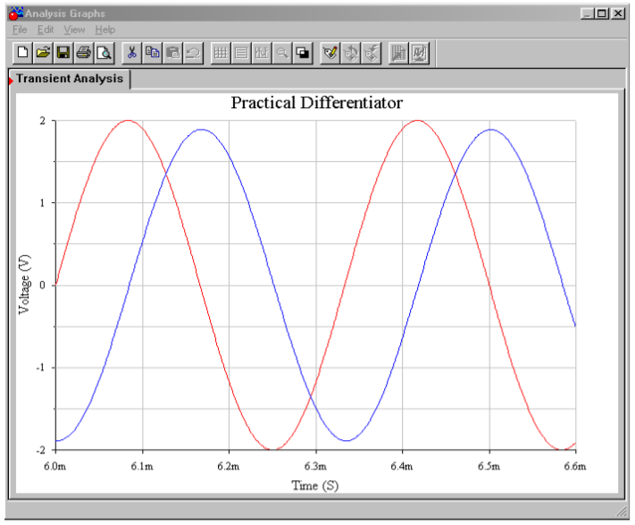
This tells us that the output waveform is also sinusoidal, but it lags the input by 90 ∘ . Note that the input frequency has not changed, but the amplitude has. The differentiator operates with a 6 dB per octave slope, thus it can be seen that the output amplitude is directly proportional to the input frequency. If this example is rerun with a frequency of 6 kHz, the output amplitude will be double the present value.
Computer Simulation
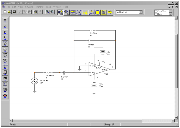
The Multisim simulation for the circuit of Example 10.3.1 is shown in Figure 10.3.10 . Note the excellent correlation for both the phase and amplitude of the output. As was the case with the integrator simulation, the Transient Analysis output plot is started after the initial conditions have settled.
Analyzing Differentiators with the Time-Discrete Method
For more complex waveforms, it is sometimes expedient to break the waveform into discrete chunks, differentiate each portion, and then combine the results. The idea is to break the waveform into equivalent straight-line segments. Differentiation of a straight-line segment will result in a constant (i.e., the slope, which does not change over that time). The process is repeated until one cycle of the input waveform is completed. The resultant levels are then joined together graphically to produce the output waveform.
Often, waveforms are symmetrical, and only part of the calculation need be performed: a sign change is all that will be needed for the mirror image portions. As an example, a triangle wave may be broken into a positive-going line segment and a negative going-line segment. The slopes should be equal, only the direction (i.e., sign) has changed. A square wave may be broken into four parts: a positive-going edge, a static positive value, a negative-going edge, and a static negative value. The “flat” portions have a slope of zero, so only one calculation must be performed, and that’s the positive-going edge. We shall take a look at both of these waveforms in the next two examples.
Example 10.3.2
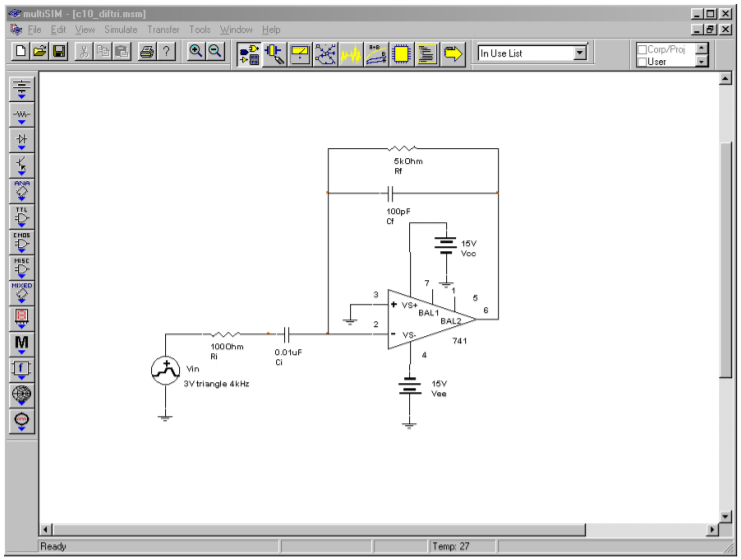
Sketch the output waveform for the circuit of Figure 10.3.9 if the input is a 3 volt peak triangle wave at 4 kHz.
First, note that the input frequency is well within the useful range of this circuit, as calculated in Example 10.3.1 . (Note that the highest harmonics will still be out of range, but the error introduced will be minor.)
The triangle wave may be broken into a positive-going portion and a negative-going portion. In either case, the total voltage change will be 6 V in one half-cycle. The period of the waveform is
![]()
![]()
Therefore, for the positive going portion, a 6 volt change will be seen in 125 𝜇 s (−6 V in 125 𝜇 s for the negative going portion). The slope is
![]()
![]()
Which, as a time-domain expression is
![]()
Substituting this Equation into Equation 10.3.1 yields
![]()
[V_{out}(t) = -5 k \times 10 nF \frac{d 48000 t}{dt} \]
[V_{out}(t) = -2.4 V \]
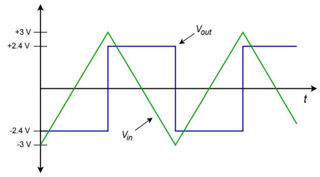
During 𝑡=0 through 𝑡=125𝜇 s, the output is −2.4 V. Differentiation of the second half of the wave is similar, but produces a positive output, +2.4 V. The result is a 4 kHz square wave that is 2.4 V peak. The resulting waveform is shown in Figure 10.3.11 .
Computer Simulation
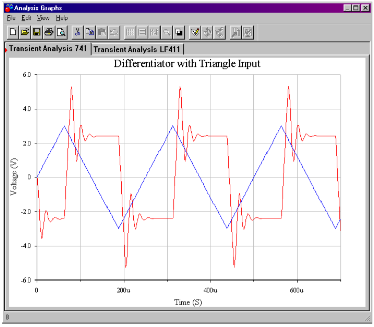
Some circuits are more sensitive to the choice of op amp than others are, and the effects of an improper choice may not always be immediately apparent without first building or simulating the circuit. A good example of this is shown in Figure 10.3.12 . Multisim was used to create the Transient Analysis for the circuit of Example 10.3.2 with two different op amps. Accurate differentiation requires excellent high frequency response from the op amp. In the first simulation, a 741 op amp is used. This device is not particularly fast. As a result, the output waveform suffers from excessive overshoot and ringing. Also, slew rate limiting is fairly obvious, slowing the transitions of the output waveform. In contrast, using an LF411 in the same circuit yields far superior response. Some overshoot still exists, but its magnitude has been restrained, as has the ringing. Also, slew rate limiting is reduced by a wide margin. Clearly, the second result is much closer to the ideal calculation than the first run.

Example 10.3.3
Repeat Example 10.3.2 with a 3 V peak, 4 kHz square as the input. Assume that the rising and falling edges of the square wave have been slew limited to 5 V/ 𝜇 s.
During the time periods that the input is at ±3 V, the output will be zero. This is because the input slope is, by definition, zero when the signal is “flat”. An output is only noted during the transitions between the ±3 V levels. Therefore, we need to find the slope of the transitions. It was stated that due to slew rate limiting (perhaps from some previous amplifier stage) the transitions run at 5 V/ 𝜇 s. As a time-domain expression, this is
![]()
Substituting this Equation into Equation 10.3.1 yields,
![]()
![]()
![]()
Obviously, when using a standard op amp and ±15 V power supply, clipping will occur in the vicinity of −13.5 V. For the negative going edge, a similar result will be seen (+250 V calculated, with clipping at +13.5 V). The resulting waveform is shown in Figure 10.3.13 . Note that the output waveform spikes will also be limited by the slew rate of the differentiator’s op amp.

Example 10.3.4
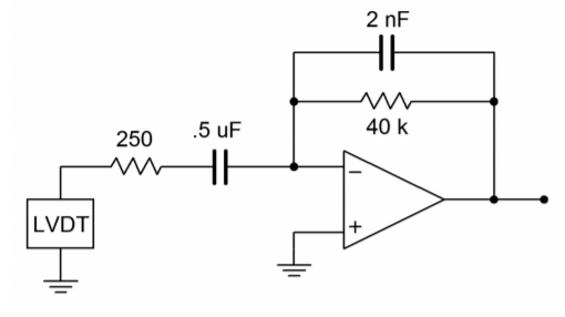
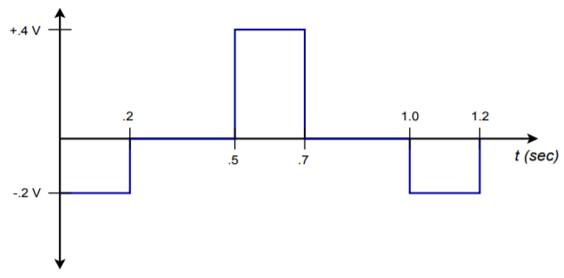
Figure 10.3.14 shows a differentiator receiving a signal from an LVDT, or linear variable differential transformer.[1] An LVDT can be used to accurately measure the position of objects with displacements of less than one-thousandth of an inch. This could be useful in a computer-aided manufacturing system. By differentiating this position signal, a velocity signal may be derived. A second differentiation will produce acceleration. If the LVDT produces the wave shown in Figure 10.3.14 , determine the velocity/time curve for the object being tracked.
First, check the upper frequency limit for the circuit.
![]()
![]()
![]()
![]()
![]()
![]()
The limit will be the lower of the two, or 1.273 kHz. This is well above the slowly changing input signal, and therefore, high accuracy should be possible.
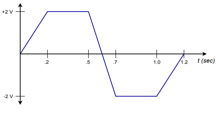
This wave can be analyzed in piece-wise fashion. The ramp portions will produce constant output levels and the flat portions will produce an output of 0 V (i.e., the rate of change is zero).
For the first section,
![]()
![]()
Which, as a time-domain expression, is
![]()
![]()
![]()
![]()
So, during 𝑡=0 through 𝑡=0.2 s, the output is −0.2 V. The time period between 0.2 s and 0.5 s will produce an output of 0 V. For the negative-going portion,
![]()
![]()
![]()
![]()
![]()
![]()
The output is 0.4 V between 0.5 s and 0.7 s. The third section has the same slope as the first section, and will also produce a −0.2 V level. The output waveform is drawn in Figure 10.3.15 .
- An LVDT is a transformer with dual secondary windings and a movable core. The core is connected to a shaft, that is in turn actuated by some external object. The movement of the core alters the mutual inductance between primary and secondary. A carrier signal is fed into the primary, and the changing mutual inductance alters the strength of the signal induced into the secondaries. This signal change is turned into a simple DC voltage by a demodulator. The resulting DC potential is proportional to the position of the core, and thus, proportional to the position of the object under measurement. ↵

