
1.2 JFET Internals
A simplified internal model of a JFET is shown in Figure 1.2.1. The main portion of the device is called the channel. The diagram illustrates an N-channel device. The channel is built upon a substrate (i.e., base layer) of oppositely doped material. Attached to the opposing ends of the channel are two terminals; the source and the drain. Embedded within the channel is a region using the opposite material type. A lead is attached to this as well and is called the gate. Although there is not perfect correspondence between them, the drain, source and gate are roughly analogous to the BJT’s collector, emitter and base, respectively.
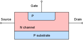
This diagram is drawn symmetrically. Some devices are designed in this fashion and their drain and source terminals can be swapped with no change in operation. This is not true for all devices, though. For small values of drain-source voltage, the channel exhibits a certain amount of resistance that is dependent on the doping level and physical layout of the device. Further, under normal operation, 𝐼𝐷 will equal 𝐼𝑆.
To understand how the device behaves, refer to Figure 1.2.2. Here we shall consider electron flow (shown as a dashed line). First, a positive voltage, 𝑉𝐷𝐷, is attached to the drain terminal along with a current limiting resistor, 𝑅𝐷. A negative supply, 𝑉𝐺𝐺, is applied to the gate terminal via resistor 𝑅𝐺. Let’s start with the gate supply set to zero. If we start 𝑉𝐷𝐷 at zero, here is what happens as we increase its value. Initially, an increase in drain-source voltage will elicit a proportional increase in the current flowing through the channel. In other words, the channel acts like a resistor. As the voltage across the drain-source increases further, at some point the current will saturate, and no further increases in current will occur in spite of further increases in 𝑉𝐷𝐷 and 𝑉𝐷𝑆. At this point the device is behaving as a constant current source. The drain-source voltage where this transition occurs is called the pinch-off voltage, 𝑉𝑝. If the drain-source voltage increases too much, breakdown will occur and current will begin to increase rapidly.
What’s particularly interesting is what happens when the gate supply is increased in the negative direction. This reverse-biases the gate-source PN junction and results in a larger depletion region being formed. The depletion region widens into the channel, thus restricting current flow sooner and at a lower level. The more negative we make 𝑉𝐺𝐺, the lower 𝐼𝐷 becomes. Eventually, when 𝑉𝐺𝐺 goes negative enough, the drain current will turn off. This voltage is called 𝑉𝐺𝑆(𝑜𝑓𝑓) and it has the same magnitude as 𝑉𝑃 (i.e., 𝑉𝑃=|𝑉𝐺𝑆(𝑜𝑓𝑓)|). The action can be thought of as operating like a water valve: turning the gate source voltage more negative is like turning off the spigot and decreasing the flow.

The operation of the JFET can visualized nicely by plotting a set of drain curves, as shown in Figure 1.2.3.
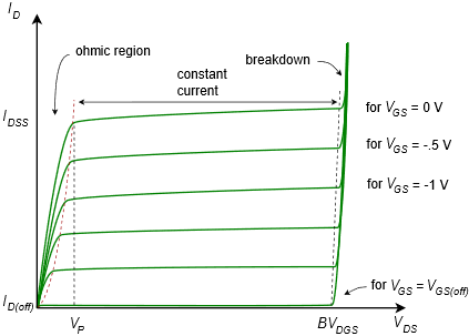
The drain curve family plots drain current, 𝐼𝐷, versus drain-source voltage, 𝑉𝐷𝑆. We begin with the top-most curve. This is generated by setting the gate-source voltage, 𝑉𝐺𝑆, to zero. We then cycle 𝑉𝐷𝑆 from zero to some higher value. Initially, we see a proportional rise in 𝐼𝐷 as 𝑉𝐷𝑆 increases. This is called the ohmic or triode region. Eventually, the channel saturates and the current levels out. This is the constant current or saturation region and it occurs for 𝑉𝐷𝑆>𝑉𝑃. The breakdown voltage is called 𝐵𝑉𝐷𝐺𝑆, or alternately, 𝑉(𝐵𝑅)𝐷𝑆. Above this voltage the current increases rapidly. As usual, we do not wish to operate the device in this breakdown region.
If we now repeat the process but this time use a small negative value for 𝑉𝐺𝑆, we will trace out a curve of very similar shape. The transition to constant current mode will happen at a slightly lower voltage and the current value will be somewhat lower as well. This process continues in like fashion as we make 𝑉𝐺𝑆 more and more negative. Eventually, when 𝑉𝐺𝑆=𝑉𝐺𝑆(𝑜𝑓𝑓), the drain current drops to virtually zero (in fact, a small leakage current flows called 𝐼𝐷(𝑜𝑓𝑓)). In contrast, if 𝑉𝐺𝑆 was allowed to go positive, operation would be lost because the PN junction would become forward-biased and we would lose control of the current via the depletion region. This means that the JFET’s current control is entirely in the second quadrant and the largest drain current flows when 𝑉𝐺𝑆=0 V. This current is called 𝐼𝐷𝑆𝑆, which stands for the drain current with a shorted gate-source (i.e, if it’s shorted, then 𝑉𝐺𝑆=0 V). The JFET cannot produce a continuous current larger than 𝐼𝐷𝑆𝑆 safely.
The characteristic equation relating drain current and gate-source voltage is shown below. This is valid for the constant current region (i.e., 𝑉𝐷𝑆>𝑉𝑃).
![\[I_D = I_{DSS} \left( 1 - \frac{V_{GS}}{V_{GS (off )}} \right)^2 \]](https://pressbooks.nscc.ca/app/uploads/quicklatex/quicklatex.com-e385c0981c41e62126e8dfe37359350c_l3.png "Rendered by QuickLaTeX.com")
(1.2.1)
Where
𝑉𝐺𝑆 is the gate-source voltage (𝑉𝐺𝑆(𝑜𝑓𝑓)≤𝑉𝐺𝑆≤0),
𝐼𝐷 is the drain current,
𝐼𝐷𝑆𝑆 is the maximum current,
𝑉𝐺𝑆(𝑜𝑓𝑓) is the turn-off voltage.
From this we see that the JFET is a square-law device rather than like the BJT which has a logarithmic characteristic.[1] In essence, this curve is a portion of a parabola. This means that the JFET’s characteristic curve is much more gradual in slope than that of a BJT. This will have important implications when it comes to voltage gain potential and distortion, as we shall see in the following chapter.
It is useful to remember that 𝑉𝐺𝑆(𝑜𝑓𝑓) and 𝐼𝐷𝑆𝑆 are unique to a given device, rather like 𝛽 is for a BJT. There can also be a fairly large variation in these parameters. For example, a particular model of JFET might show an 𝐼𝐷𝑆𝑆 variation between 2 mA and 20 mA, and a 𝑉𝐺𝑆(𝑜𝑓𝑓) variation between −2 V and −8 V. Generally, the most negative 𝑉𝐺𝑆(𝑜𝑓𝑓) values will be associated with the largest 𝐼𝐷𝑆𝑆 values.
Equation 1.2.1 is plotted in Figure 1.2.4. Compare this curve to the curve generated by the Shockley equation for BJTs, Figure 7.2.1. The graph is shown in normalized form. Instead of plotting for specific values of 𝑉𝐺𝑆(𝑜𝑓𝑓) and 𝐼𝐷𝑆𝑆, the axes are presented as fractional portions of the maximums (i.e., the horizontal axis is −𝑉𝐺𝑆/𝑉𝐺𝑆(𝑜𝑓𝑓) and the vertical axis is 𝐼𝐷/𝐼𝐷𝑆𝑆).

Example 1.2.1
Using both Equation 1.2.1 and the graph of Figure 1.2.4, determine the drain current if the gate-source voltage is −1 V and the JFET specs are 𝐼𝐷𝑆𝑆 = 8 mA and 𝑉𝐺𝑆(𝑜𝑓𝑓) = −2 V.
First, using Equation 1.2.1
![\[I_D = 8mA \left( 1 - \frac{-1V}{-2V} \right)^2 \]](https://pressbooks.nscc.ca/app/uploads/quicklatex/quicklatex.com-8073262ce2099806998d78542fcca2a6_l3.png "Rendered by QuickLaTeX.com")
![\[I_D = 2 mA \]](https://pressbooks.nscc.ca/app/uploads/quicklatex/quicklatex.com-eec130dcb7e8627f7fb7db700cdf7764_l3.png "Rendered by QuickLaTeX.com")
Using the graph, 𝑉𝐺𝑆/𝑉𝐺𝑆(𝑜𝑓𝑓)is 1 V/−2 V, or −0.5. Find this value on the horizontal axis, follow up to the curve and then across to the right vertical axis. The normalized drain current is 0.25, thus 𝐼𝐷 is 0.25 𝐼𝐷𝑆𝑆, or 2 mA.
As the characteristic curve plots output current versus input voltage, the slope of this represents the transconductance, an important characteristic for biasing and signal analysis. Device transconductance is denoted as 𝑔𝑚, or alternately as 𝑔𝑓𝑠, and given units of siemens. We can derive an equation for transconductance by taking the derivative of Equation 1.2.1.
![\[\frac{d I_D}{d V_{GS}} =-\frac{2 I_{DSS}}{V_{GS (off )}} \left( 1 - \frac{V_{GS}}{V_{GS (off )}} \right) \]](https://pressbooks.nscc.ca/app/uploads/quicklatex/quicklatex.com-48cda7227760418e5908e3b877aa525b_l3.png "Rendered by QuickLaTeX.com")
The coefficient −2𝐼𝐷𝑆𝑆/𝑉𝐺𝑆(𝑜𝑓𝑓) is defined as 𝑔𝑚0, the transconductance when 𝑉𝐺𝑆=0V. This is the maximum transconductance of the device. Substituting, we arrive at
![\[g_{m0} =- \frac{2 I_{DSS}}{V_{GS(off )}} \]](https://pressbooks.nscc.ca/app/uploads/quicklatex/quicklatex.com-e93d435cc5258e1422e1e601424cc52a_l3.png "Rendered by QuickLaTeX.com")
(1.2.2)
![\[g_m = g_{m0} \left( 1 − \frac{V_{GS}}{V_{GS (off )}} \right) \]](https://pressbooks.nscc.ca/app/uploads/quicklatex/quicklatex.com-5df8457035d3d877e01923c1e451bfd6_l3.png "Rendered by QuickLaTeX.com")
(1.2.3)

A normalized plot of transconductance versus 𝑉𝐺𝑆 is shown in Figure 1.2.5. The horizontal axis is −𝑉𝐺𝑆/𝑉𝐺𝑆(𝑜𝑓𝑓) and the vertical axis is 𝑔𝑚/𝑔𝑚0.
From this graph we see that the transconductance is a linear function.
Another item of interest regarding these device equations: If we combine Equations 1.2.1 and 1.2.3, we generate two equations that will prove useful in upcoming work.
![\[\frac{g_m}{g_{m0}} = \sqrt{\frac{I_D}{I_{DSS}}} \]](https://pressbooks.nscc.ca/app/uploads/quicklatex/quicklatex.com-d6614446d520ef15ec21b065680e09a0_l3.png "Rendered by QuickLaTeX.com")
(1.2.4)
(1.2.5)
Before moving on, the schematic symbols for JFETs are shown in Figure 1.2.6. The middle vertical line represents the channel, and as is usually the case, the arrow points to N material. Sometimes the gate arrow is draw in the middle rather than toward the source. Also, as is the case the BJT, sometimes these symbols are drawn within a circle.

- As evidenced in the Shockley equation, Equation 2.1.1. ↵
