
5.2 Class D Basics
The key to the high efficiency of class D operation is to only operate the output devices as switches. That is, they are operated at the extreme ends of the load line, in either cutoff or saturation. The only exception to this rule is when the output device is transitioning from one state to another. Either BJTs or E-MOSFETs can be used, although for reasons that we shall examine, E-MOSFETs tend to be preferred in many applications and therefore we shall use them here as a general rule.
To understand the power advantage of class D switching, consider the circuit of Figure 5.2.1 . Here we have an E-MOSFET being driven by a square wave at its gate terminal. The square wave runs from zero to some voltage well above 𝑉𝐺𝑆(𝑡ℎ) , sufficient to fully turn-on the MOSFET.
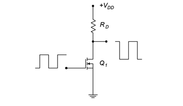
At the drain, an inverted square wave appears that ideally runs from +𝑉𝐷𝐷 down to zero volts. When the MOSFET is off, no drain current flows. Therefore, the drop across the drain resistor, 𝑅𝐷 , is zero. Consequently, by KVL, 𝑉𝐷𝑆 must equal 𝑉𝐷𝐷 . When the gate signal goes high, it turns on the MOSFET causing a large current. Ideally, this current equals 𝑉𝐷𝐷/𝑅𝐷 and 𝑉𝐷𝑆=0 V. In reality, the MOSFET will present some resistance (𝑟𝐷𝑆(𝑜𝑛)) and this essentially creates a voltage divider between the device and 𝑅𝐷. Obviously, if 𝑟𝐷𝑆(𝑜𝑛)≪𝑅𝐷 then we can approximate the low state as zero volts.
In the ideal case, the transistor dissipates no power. Here’s why: When the gate is low, the device is off so no current flows. Although the device voltage is very high, the product of the device’s voltage and current is zero. When the gate is high, the transistor turns on and conducts maximum current, however, the voltage across the device is zero, and the resulting product is zero once again. Therefore, the device dissipates no power.
The reality of the situation reveals that some power is indeed wasted by the output device. There are two chief culprits: non-zero turn-on voltage (caused by 𝑟𝐷𝑆(𝑜𝑛) for example) and state transitions that are not instantaneous (i.e., the rise and fall times of the waveforms are not zero). These effects are illustrated in Figure 5.2.2 .
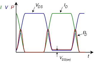
The rise and fall times are exaggerated for clarity as is the voltage drop across the transistor. The green curve represents the device current while the blue curve indicates the device voltage. Note that during the on-state the transistor voltage is not zero, although it is very small. The product of these two curves is the power dissipated by the transistor and is shown in red. In the off-state, no power is dissipated. In the on-state, a small amount of power is dissipated due to the device’s on-voltage. Power spikes also occur at the state transitions as neither the current nor the voltage are at zero.
The area under the red curve represents the total power dissipated by the output transistor. In order to minimize this loss and maximize the efficiency, we would like as low of an 𝑟𝐷𝑆(𝑜𝑛) as possible along with very fast switching speeds. As power EMOSFETs tend to switch faster than their BJT counterparts, this presents a compelling argument for their use. Further, large power E-MOSFETs may exhibit 𝑟𝐷𝑆(𝑜𝑛) values of just a few milliohms, guaranteeing relatively small on-state losses (compared to load power) even with drain currents of several tens of amps.
