
11.5 Offsets
Offsets are undesirable DC levels appearing at the output of a circuit. If op amps were perfect, there would be no such thing as an offset. Even though part matching is very close when ICs are made, the parts will not be identical. One possible example is the fact that the transistors used for the differential amplifier stage will not have identical characteristics. Because of this, their DC bias points are slightly different. This difference, or unbalance, is amplified by the remaining stages and will eventually produce a DC voltage at the output. Because all op amps are slightly different, you never know what the exact output offset will be. For measurement applications, this offset creates uncertainty in readings. For example, if the circuit output measures 100 mV, the signal might be 99 mV with 1 mV of offset. It might also be 101 mV with -1mV offset. In other applications, offsets can harm following stages or loads. Dynamic loudspeakers and headphones are two loads that should not be fed DC signals. This will reduce their maximum volume and increase their distortion. In short, offsets are not desired. Let’s see what the causes are and how we can reduce or eliminate their effect.
Offset Sources and Compensation
For bipolar input sections the major cause of input current mismatch is the variation of beta. Base-emitter junction voltage variation is the major cause of input voltage deviation. For field effect devices, current variation is much less of a problem as the magnitude of input current is very low to begin with. Unfortunately, FETs do suffer from larger input voltage variations due to transconductance curve mismatches.
As mentioned in Chapter Two, the input current into the bases (or gates, in the case of an FET) of the first stage is called 𝐼𝐵 , the input bias current. In reality, this is an average of the two input currents, 𝐼𝐵+ and 𝐼𝐵− . The magnitude of their difference is called the input offset current, 𝐼𝑂𝑆 (some manufacturers use the symbol 𝐼𝐼𝑂 ). Note that the actual direction of 𝐼𝐵 is normally not specified, but can usually be determined from the manufacturer’s circuit diagram. 𝐼𝐵 flows into the op amp if the input devices are NPN, and out of the op amp if the input devices are PNP.
![\[I_B = \frac{I_{B+} + I_{B-}}{2} \]](https://pressbooks.nscc.ca/app/uploads/quicklatex/quicklatex.com-98387dc1e83d76dba63b900041727e85_l3.png "Rendered by QuickLaTeX.com")
![\[I_{OS} = | I_{B+} - I_{B-} | \]](https://pressbooks.nscc.ca/app/uploads/quicklatex/quicklatex.com-51743cb664e7239ae150a8bc7b5c1ba7_l3.png "Rendered by QuickLaTeX.com")
(5.5.1)
The voltage difference for the input stage is referred to as the input offset voltage, 𝑉𝑂𝑆 (some manufacturers use the symbol 𝑉𝐼𝑂 ). This is the potential required between the two inputs to null the output, that is, to re-align the output to 0 V DC. Both 𝐼𝑂𝑆 and 𝑉𝑂𝑆 are available on data sheets. The absolute magnitude of these offsets generally gets worse at temperature extremes. Table 5.5.1 shows some typical values. Note the low 𝐼𝐵 and 𝐼𝑂𝑆 values for the FET input 411.
| Device |
|---|
| 𝐼𝐵 |
| 𝐼𝑂𝑆 |
| 𝑉𝑂𝑆 |
| 5534 |
| 800 nA |
| 10 nA |
| 0.5 mV |
| 411 |
| 50 pA |
| 25 pA |
| 0.8 mV |
| 318 |
| 150 nA |
| 30 nA |
| 4 mV |
| 741 |
| 80 nA |
| 20 nA |
| 1 mV |
Table 11.5.1
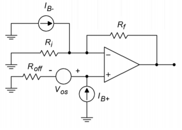
Remember, these numbers are absolutes, so when 𝐼𝑂𝑆 is specified as 10 nA, it means that the actual 𝐼𝑂𝑆 can be anywhere between -10 nA and +10 nA. 𝐼𝐵 , 𝐼𝑂𝑆 and 𝑉𝑂𝑆 combine with other circuit elements to produce an output offset voltage. As this is a linear circuit, superposition may be used to separately calculate their effects. The model in Figure 5.5.1 will be used. 𝑅𝑖 and 𝑅𝑓 are the standard feedback components, and 𝑅𝑜𝑓𝑓 is called the offset compensation resistor (in some cases it may be zero). Because the input signal is grounded, this model is valid for both inverting and noninverting amplifiers.
𝑉𝑂𝑆 is seen as a small input voltage and is multiplied by the circuit’s noise gain in order to find its contribution to the output offset. Offsets are by nature DC, so it is important to use the DC noise gain. Consequently, any capacitors found within the feedback loop should be mathematically “opened” for this calculation (for example, when working with the filter circuits presented in Chapter Eleven)
![\[V_{out−offset 1} = A_{noise} V_{OS} \]](https://pressbooks.nscc.ca/app/uploads/quicklatex/quicklatex.com-12e5ecfab1a21092de24e209de09b0e2_l3.png "Rendered by QuickLaTeX.com")
(5.5.2)
where
![\[A_{noise} = 1+ \frac{R_f}{R_i} = \frac{R_i+R_f}{R_i} \]](https://pressbooks.nscc.ca/app/uploads/quicklatex/quicklatex.com-17cf0f84cad59a641e6de3913e382206_l3.png "Rendered by QuickLaTeX.com")
𝐼𝐵 and 𝐼𝑂𝑆 pass through input and feedback resistors to produce their output contributions. First, consider the effect of 𝐼𝐵+ . This creates a voltage across 𝑅𝑜𝑓𝑓 . This voltage is then multiplied by the circuit noise gain to yield its portion of the output offset.
![\[V_{out -offset 2} = I_{B+} R_{off} A_{noise} \]](https://pressbooks.nscc.ca/app/uploads/quicklatex/quicklatex.com-19297738e10ecb0659d084633a67a151_l3.png "Rendered by QuickLaTeX.com")
(5.5.3)
For 𝐼𝐵− , recall that the inverting input is at virtual ground. This implies that the voltage across 𝑅𝑖 must be zero, and therefore, the current through 𝑅𝑖 must be zero. Consequently, all of 𝐼𝐵− flows through 𝑅𝑓 . This creates a relative negative potential at the output.
![\[V_{out -offset 3} = −I_{B-} R_f \]](https://pressbooks.nscc.ca/app/uploads/quicklatex/quicklatex.com-f9d68020d4acbe1ca63905f1114e7660_l3.png "Rendered by QuickLaTeX.com")
(5.5.4)
So the combination of the input bias current effects is:
![\[V_{out -offset(I_B)} = | I_{B+} R_{off} A_{noise} - I_{B-} R_f | \]](https://pressbooks.nscc.ca/app/uploads/quicklatex/quicklatex.com-549ac8ad1fb6e60038eb2bc7dfbe1cc4_l3.png "Rendered by QuickLaTeX.com")
(5.5.5)
Expanding this produces
![\[V_{out -offset(I_B)} = I_{B+} R_{off} \frac{R_i+R_f}{R_i} - I_{B-} R_f \]](https://pressbooks.nscc.ca/app/uploads/quicklatex/quicklatex.com-b8b0a74f5d5cb7d53f9535944fea091f_l3.png "Rendered by QuickLaTeX.com")
![\[V_{out -offset(I_B)} = \left( I_{B+} R_{off} \frac{R_i+R_f}{R_i R_f} −I_{B-}\right) R_f \]](https://pressbooks.nscc.ca/app/uploads/quicklatex/quicklatex.com-b906907addd417b305f29b23feaf8137_l3.png "Rendered by QuickLaTeX.com")
By noting the product-sum rule for resistor combination 𝑅𝑖 , 𝑅𝑓 , this can be further simplified to
![\[V_{out -offset(I_B)} = \left(\frac{I_{B+} R_{off}}{R_i || R_f} −I_{B-}\right) R_f \]](https://pressbooks.nscc.ca/app/uploads/quicklatex/quicklatex.com-790d1292f35bd9d74dba5407eab21870_l3.png "Rendered by QuickLaTeX.com")
(5.5.6)
If 𝑅𝑜𝑓𝑓 is set to equal 𝑅𝑖||𝑅𝑓 , this reduces to:
![\[V_{out -offset(I_B)} = (I_{B+} - I_{B-} )R_f \]](https://pressbooks.nscc.ca/app/uploads/quicklatex/quicklatex.com-f02b289a9efeea5c62de978702277f24_l3.png "Rendered by QuickLaTeX.com")
By definition,
so we finally come to
![\[V_{out-offset(I_B)} = I_{OS} R_f \]](https://pressbooks.nscc.ca/app/uploads/quicklatex/quicklatex.com-d166eb13ddf2aa136ee4a2030d5f0865_l3.png "Rendered by QuickLaTeX.com")
(5.5.7)
If it is possible, 𝑅𝑜𝑓𝑓 should be set to 𝑅𝑖||𝑅𝑓 . This drastically reduces the effect of the input bias current. Note that the value of 𝑅𝑜𝑓𝑓 includes the driving source internal resistance. If 𝑅𝑖||𝑅𝑓=2𝑘Ω and the driving source resistance is 100 Ω , the required resistance value would be 1.9 k Ω . If setting 𝑅𝑜𝑓𝑓 to the optimum value is not possible, you can at least reduce the effect of 𝐼𝐵 by using a partial value. Also, note that it is possible to determine the polarity of the offset caused by 𝐼𝐵+ and 𝐼𝐵− (Equation 5.5.6 ) if actual currents and the type of device used in the diff amp stage are known. The circuit of Figure 5.5.1 assumes that NPN devices are being used, hence the currents are drawn as entering the op amp. PNP input devices would produce the opposite polarity. Typically, though, we don’t have precise values for 𝐼𝐵+ and 𝐼𝐵− , and thus can only compute the worst-case magnitude.
For a final result, we may combine our components:
![\[V_{out-offset} = V_{OS} A_{noise} + I_{OS} R_f \]](https://pressbooks.nscc.ca/app/uploads/quicklatex/quicklatex.com-4cd928912d6238a81958c04e0b200239_l3.png "Rendered by QuickLaTeX.com")
(5.5.8)
if 𝑅𝑜𝑓𝑓=𝑅𝑖||𝑅𝑓 , and
![\[V_{out-offset} = V_{OS} A_{noise} +|I_{B+} R_{off} A_{noise} - I_{B} R_f| \]](https://pressbooks.nscc.ca/app/uploads/quicklatex/quicklatex.com-87a955f84b8983034a0a9a4d6078b9bb_l3.png "Rendered by QuickLaTeX.com")
(5.5.9)
if 𝑅𝑜𝑓𝑓≠𝑅𝑖||𝑅𝑓 .
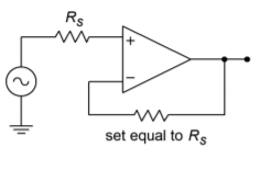
There is one special case involving the selection of Roff, and that deals with a voltage follower. Normally for a follower, 𝑅𝑓=0Ω . What if the driving source resistance is perhaps 0 Ω ? The calculation would require an 𝑅𝑜𝑓𝑓 of 0 Ω , and thus a -50 Ω resistor to compensate for the source resistance. This is of course, impossible! To compensate for the 50 Ω source, use 50 Ω for 𝑅𝑓 . The circuit gain will still be unity, but 𝐼𝐵 will now be compensated for. This is shown in Figure 5.5.2 .
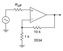
Example 5.5.1
Determine the typical output offset voltage for the circuit of Figure 5.5.3 if 𝑅𝑜𝑓𝑓 is 0 Ω . Then determine an optimum size for 𝑅𝑜𝑓𝑓 and calculate the new offset.
From the data sheet for the 5534, we find 𝑉𝑂𝑆=0.5𝑚𝑉 , 𝐼𝑂𝑆=10𝑛𝐴 , and 𝐼𝐵=800𝑛𝐴 . Because this is an approximation, assume 𝐼𝐵+=𝐼𝐵−=𝐼𝐵 .
![\[A_{noise} = 1+ \frac{R_f}{R_i} \]](https://pressbooks.nscc.ca/app/uploads/quicklatex/quicklatex.com-31fc400268aeb15502371a2624efe36d_l3.png "Rendered by QuickLaTeX.com")
![\[A_{noise} = 1+ \frac{10 k}{1 k} \]](https://pressbooks.nscc.ca/app/uploads/quicklatex/quicklatex.com-0bccbff224a599e7604ccec5e29c7833_l3.png "Rendered by QuickLaTeX.com")
![\[A_{noise} = 11 \]](https://pressbooks.nscc.ca/app/uploads/quicklatex/quicklatex.com-41269a2dc311b24041582642c6cfe6b1_l3.png "Rendered by QuickLaTeX.com")
![\[V_{out -offset} = V_{OS} A_{noise} + |I_{B+} R_{off} A_{noise} - I_{B-} R_f| \]](https://pressbooks.nscc.ca/app/uploads/quicklatex/quicklatex.com-04ceefe40d77d64561d26eb966c134fb_l3.png "Rendered by QuickLaTeX.com")
![\[V_{out -offset} = 0.5mV\times 11+|800 nA\times 0\times 11-800 n A\times 10 k| \]](https://pressbooks.nscc.ca/app/uploads/quicklatex/quicklatex.com-ac971136b55794d78631dee540958077_l3.png "Rendered by QuickLaTeX.com")
![\[V_{out -offset} = 5.5mV+8mV \]](https://pressbooks.nscc.ca/app/uploads/quicklatex/quicklatex.com-81170882310d6d810f8c9b41a96da3ce_l3.png "Rendered by QuickLaTeX.com")
![\[V_{out -offset} =13.5 mV \]](https://pressbooks.nscc.ca/app/uploads/quicklatex/quicklatex.com-cb385731e3c4f429e46382ff9d9a80fe_l3.png "Rendered by QuickLaTeX.com")
Remember, this is the magnitude of the offset, it could be anywhere within ± 13.5 mV. It might be worse if this is not a typical device. Now we find the optimum offset compensating resistor:
![\[R_{off} = R_i || R_f \]](https://pressbooks.nscc.ca/app/uploads/quicklatex/quicklatex.com-f040863c2d8dfd14f441afb17e67cf28_l3.png "Rendered by QuickLaTeX.com")
![\[R_{off} = 1 k || 10 k \]](https://pressbooks.nscc.ca/app/uploads/quicklatex/quicklatex.com-963f851744438509f3c7e8c0e1af449c_l3.png "Rendered by QuickLaTeX.com")
![\[R_{off} = 909 \Omega \]](https://pressbooks.nscc.ca/app/uploads/quicklatex/quicklatex.com-e73de2ccf425ee567f765fde5903302c_l3.png "Rendered by QuickLaTeX.com")
For this case, the offset Equation reduces to
![\[V_{out-offset} = 0.5mV\times 11+10 nA\times 10 k \]](https://pressbooks.nscc.ca/app/uploads/quicklatex/quicklatex.com-1e2071d5d4f29aa70cfb7c41c4cbfdad_l3.png "Rendered by QuickLaTeX.com")
![\[V_{out-offset} = 5.5mV+100\mu V \]](https://pressbooks.nscc.ca/app/uploads/quicklatex/quicklatex.com-6bfdb19cffcd17f8b695f67e8f1c1c7f_l3.png "Rendered by QuickLaTeX.com")
![\[V_{out-offset} = 5.6mV \]](https://pressbooks.nscc.ca/app/uploads/quicklatex/quicklatex.com-0350f7de54761e936a320f38082e8adc_l3.png "Rendered by QuickLaTeX.com")
By adding 𝑅𝑜𝑓𝑓 , the output offset voltage is more than halved. This may lead you to think that it is always wise to add 𝑅𝑜𝑓𝑓 . Such is not the case. There are two times when you may prefer to leave it out: 1) to optimize noise characteristics, as we will see shortly, and 2) when using FET input op amps. FET input devices have very small input bias and offset currents to begin with, so their effect is negligible when using typical resistor values.
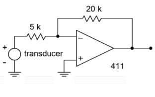
Example 5.5.2
The circuit of Figure 5.5.4 is used as part of a measurement system. Assuming that the DC input signal is 3 mV, how much uncertainty is there in the output voltage typically?
The desired output from the amplifier is
![\[V_{out} = A_v V_{in} \]](https://pressbooks.nscc.ca/app/uploads/quicklatex/quicklatex.com-06700dfd5114e55bda0c48bdf9ebeda6_l3.png "Rendered by QuickLaTeX.com")
![\[V_{out} = - \frac{R_f}{R_i} V_{in} \]](https://pressbooks.nscc.ca/app/uploads/quicklatex/quicklatex.com-e3481950576a479c1bd8028f71d06f60_l3.png "Rendered by QuickLaTeX.com")
![\[V_{out} = - \frac{20 k}{5 k} 3 mV \]](https://pressbooks.nscc.ca/app/uploads/quicklatex/quicklatex.com-13fb0314f8bdd2014d016888dc40930a_l3.png "Rendered by QuickLaTeX.com")
![\[V_{out} = -12 mV \]](https://pressbooks.nscc.ca/app/uploads/quicklatex/quicklatex.com-0f969c94915e63f46d66ee4040bbdfc6_l3.png "Rendered by QuickLaTeX.com")
The typical specs for the 411 are 𝑉𝑂𝑆=0.8𝑚𝑉 , 𝐼𝑂𝑆=25𝑝𝐴 , 𝐼𝐵=50𝑝𝐴
![\[A_{noise} = 1+ \frac{20 k}{5 k} \]](https://pressbooks.nscc.ca/app/uploads/quicklatex/quicklatex.com-dcb821308b9b6cb8ed3bb5f2f06b678e_l3.png "Rendered by QuickLaTeX.com")
![\[A_{noise} = 5 \]](https://pressbooks.nscc.ca/app/uploads/quicklatex/quicklatex.com-a2509e8f0153bd8197f2c46247f9f9ec_l3.png "Rendered by QuickLaTeX.com")
![\[V_{out -offset} = V_{OS} A_{noise} +|I_{B+} R_{off} A_{noise} - I_{B-}R_f| \]](https://pressbooks.nscc.ca/app/uploads/quicklatex/quicklatex.com-f04beb9fb4d39f471eb8db4172b64212_l3.png "Rendered by QuickLaTeX.com")
![\[V_{out -offset} = 0.8mV\times 5+| 50 pA\times 0\times 11-50 pA\times 20 k | \]](https://pressbooks.nscc.ca/app/uploads/quicklatex/quicklatex.com-0729cf3463a258b2744dac6301fe339d_l3.png "Rendered by QuickLaTeX.com")
![\[V_{out -offset} = 4 mV+1\mu V \]](https://pressbooks.nscc.ca/app/uploads/quicklatex/quicklatex.com-92f970daec434b76dad8ff15bacdbb84_l3.png "Rendered by QuickLaTeX.com")
![\[V_{out -offset} = 4 mV \]](https://pressbooks.nscc.ca/app/uploads/quicklatex/quicklatex.com-9b9f695b9c10cf59228c85f0a7e055c6_l3.png "Rendered by QuickLaTeX.com")
The output can vary by as much as ± 4 mV. As this a DC measurement system, the results are devastating. The output can be anywhere from -12 mV – 4 mV = -16 mV, to -12 mV + 4 mV = -8 mV. That’s a 2:1 spread, and it’s caused solely by the op amp. Note that the addition of 𝑅𝑜𝑓𝑓 would have little effect here. Because the 411 uses a FET input, its 𝐼𝐵 contribution is only 1 𝜇 V.
So, then, how do you keep output offsets to a minimum? First and foremost, make sure that the op amp chosen has low 𝐼𝑂𝑆 and 𝑉𝑂𝑆 ratings. Second, use the offset compensation resistor, 𝑅𝑜𝑓𝑓 . Third, keep the circuit resistances as low as possible. Finally, if the output offset is still too large, it can be reduced by manually nulling the circuit.
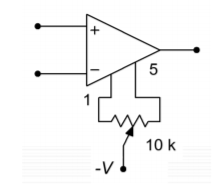
Nulling involves summing in a small signal that is of opposite polarity to the existing offset. By doing this, the new signal will completely cancel the offset and the output will show 0 V DC. This is much easier than it sounds. Most op amps have connections for null circuits. These are specified by the manufacturer and usually consist of a single potentiometer and perhaps one or two resistors. An example nulling connection is shown in Figure 5.5.5 . Usually the potentiometer is a multi-turn trim type to allow for fine adjustment. To null the circuit, the technician monitors the output with a very sensitive DC voltmeter. The input is grounded (or perhaps tied to ground through a resistor equal to the driving source resistance if it’s large). The potentiometer is then adjusted until the meter reads zero.
The drawback to this procedure is that it requires someone (or perhaps some thing) to perform the nulling. Also, the unit will require periodic adjustment to compensate for aging and environmental effects.
Computer Simulation
As stated, it is very important to match the input resistors in order to keep offsets low. This can be seen clearly in the simulation shown in Figure 5.5.6 . A noninverting voltage amplifier is modeled here using the 741. In order to focus on the offset current effect, the contribution of 𝑉𝑂𝑆 is kept small by keeping the voltage gain low. The simulation is run twice for DC Operating Point. In the case where the resistances are matched, the DC output voltage is less than 1 mV. For the unmatched case, 𝑅𝑜𝑓𝑓 is set to a fraction of an Ohm. The resulting DC output voltage is much larger at approximately 17 mV. It is worthy to note that this is approximately equal to 𝐼𝑏𝑖𝑎𝑠 times 𝑅𝑓 (80 nA times 200 k Ω ). This simulation also points out the poor performance caused by excessively large resistor values. If the simulation is re-run with the resistors scaled down in size, the offsets will be lessened.


