
4.3 MOSFET Common Drain Followers
As discussed under the section on JFETs, the common drain amplifier is also known as the source follower. The prototype amplifier circuit with device model is shown in Figure 4.3.1 . As with all voltage followers, we expect a non-inverting voltage gain close to unity with a high 𝑍𝑖𝑛 and a low 𝑍𝑜𝑢𝑡 .
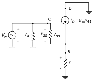
As is usual, the input signal is applied to the gate terminal and the output is taken from the source. Because the output is at the source, biasing schemes that have the source terminal grounded, such as zero bias and voltage divider bias, cannot be used.
Voltage Gain
The voltage gain equation for the common drain follower is developed as follows: We begin with the fundamental definition that voltage gain is the ratio of 𝑣𝑜𝑢𝑡 to 𝑣𝑖𝑛 , and proceed by expressing these voltages in terms of their Ohm’s law equivalents. The load is now located at the MOSFET’s source, and thus can be referred to as either 𝑟𝐿 or 𝑟𝑆 .
![\[A_v = \frac{v_{out}}{v_{i n}} = \frac{v_S}{v_G} = \frac{v_L}{v_G} \]](https://pressbooks.nscc.ca/app/uploads/quicklatex/quicklatex.com-5deb63f16d0e2a4e4e6d6f9516492c53_l3.png "Rendered by QuickLaTeX.com")
![\[ A_v = \frac{i_D r_L}{i_D r_L+v_{GS}} \]](https://pressbooks.nscc.ca/app/uploads/quicklatex/quicklatex.com-3c6ad58f60e44aae450bc432b8464cc9_l3.png "Rendered by QuickLaTeX.com")
![\[ A_v = \frac{g_m v_{GS} r_L}{g_m v_{GS} r_L+v_{GS}} \]](https://pressbooks.nscc.ca/app/uploads/quicklatex/quicklatex.com-bd0045a44f84844b76d9229671c0b8dd_l3.png "Rendered by QuickLaTeX.com")
![\[ A_v = \frac{g_m r_L}{g_m r_L+1} \]](https://pressbooks.nscc.ca/app/uploads/quicklatex/quicklatex.com-35db2a47bb2d1d27062ed7ade9d004f8_l3.png "Rendered by QuickLaTeX.com")
(4.3.1)
or, if preferred
![\[A_v = \frac{g_m r_S}{g_m r_S+1} \]](https://pressbooks.nscc.ca/app/uploads/quicklatex/quicklatex.com-c37b6d7d8a2f76ced25c59600ce7bb33_l3.png "Rendered by QuickLaTeX.com")
If 𝑔𝑚𝑟𝑆≫1 , the voltage gain will be very close to unity; a desired outcome.
Input Impedance
The analysis for source follower’s input impedance is virtually identical to that for the common source amplifier. The same commentary applies regarding the simplification of gate biasing resistors to arrive at the value of 𝑟𝐺 .
![\[Z_{in} = r_G || r_{GS} \approx r_G \]](https://pressbooks.nscc.ca/app/uploads/quicklatex/quicklatex.com-5b573d5163aed2db214df30723e798de_l3.png "Rendered by QuickLaTeX.com")
(4.3.3)
Output Impedance
In order to determine the output impedance, we modify the circuit of Figure 4.3.1 by separating the load resistance from the source bias resistor. This is shown in Figure 4.3.2 .

Looking back into the source from the perspective of the load we find that the source biasing resistor, 𝑅𝑆, is in parallel with the impedance looking back into the source terminal.
![\[Z_{out} = R_S || Z_{source} \]](https://pressbooks.nscc.ca/app/uploads/quicklatex/quicklatex.com-9cc757ee947a8eecb390f976d80b2af5_l3.png "Rendered by QuickLaTeX.com")
To find 𝑍𝑠𝑜𝑢𝑟𝑐𝑒 , note that the voltage at the source is 𝑣𝐺𝑆 and the current entering this node is 𝑖𝐷 . The ratio of the two will yield the impedance looking back into the source.
![\[Z_{source} = \frac{v_{GS}}{i_D} \]](https://pressbooks.nscc.ca/app/uploads/quicklatex/quicklatex.com-efc323a3577b75b9cf6b8cf964fcf0eb_l3.png "Rendered by QuickLaTeX.com")
![\[Z_{source} = \frac{v_{GS}}{g_m v_{GS}} \]](https://pressbooks.nscc.ca/app/uploads/quicklatex/quicklatex.com-2e3fb8041dd04fc75136f2aa43c0c2ab_l3.png "Rendered by QuickLaTeX.com")
![\[Z_{source} = \frac{1}{g_m} \]](https://pressbooks.nscc.ca/app/uploads/quicklatex/quicklatex.com-63e6bb50806d11148f771af15cd10032_l3.png "Rendered by QuickLaTeX.com")
(4.3.4)
Therefore, the output impedance is
![\[Z_{out} = R_S || \frac{1}{g_m} \]](https://pressbooks.nscc.ca/app/uploads/quicklatex/quicklatex.com-92cdead2c55f21c884eed4d1b987dec4_l3.png "Rendered by QuickLaTeX.com")
(4.3.5)
Looking at Equation 4.3.5 it is obvious that the higher the transconductance, the lower the output impedance. As noted earlier, a large transconductance also means that the voltage gain will be close to unity. As a general rule then, a large transconductance is desired for the source follower.
Time for a few illustrative examples.
Example 4.3.1
For the circuit of Figure 4.3.3 , determine the voltage gain and input impedance. Assume 𝑉𝐺𝑆(𝑜𝑓𝑓) = −0.8 V and 𝐼𝐷𝑆𝑆 = 30 mA.
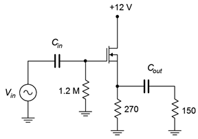
This amplifier uses self bias so we need to determine 𝑔𝑚0𝑅𝑆 .
![\[g_{m0} =- \frac{2 I_{DSS}}{V_{GS (off )}} \]](https://pressbooks.nscc.ca/app/uploads/quicklatex/quicklatex.com-b77a0a7208e012f3272aba5fd5232900_l3.png "Rendered by QuickLaTeX.com")
![\[g_{m0} =- \frac{2 \times 30mA}{-0.8 V} \]](https://pressbooks.nscc.ca/app/uploads/quicklatex/quicklatex.com-16118a562e29fa05c05de37b47ec9a0c_l3.png "Rendered by QuickLaTeX.com")
![\[g_{m0} = 75mS \]](https://pressbooks.nscc.ca/app/uploads/quicklatex/quicklatex.com-5faa63045f4fe9a3adfb393aa5687cba_l3.png "Rendered by QuickLaTeX.com")
The DC source resistance is the 270 Ω biasing resistor resulting in 𝑔𝑚0𝑅𝑆 = 16.2. From the self bias equation or graph this produces a drain current of 2.61 mA.
![\[g_m = g_{m0} \sqrt{\frac{I_D}{I_{DSS}}} \]](https://pressbooks.nscc.ca/app/uploads/quicklatex/quicklatex.com-25dac375b04238992e96ec5b62b10c9c_l3.png "Rendered by QuickLaTeX.com")
![\[g_m = 75 mS \sqrt{\frac{2.61 mA}{30 mA}} \]](https://pressbooks.nscc.ca/app/uploads/quicklatex/quicklatex.com-dbf1359c4f9ca5ae72007d3b1288409d_l3.png "Rendered by QuickLaTeX.com")
![\[g_m = 22.1mS \]](https://pressbooks.nscc.ca/app/uploads/quicklatex/quicklatex.com-8e8e55dfa27440f9a893b40b9344cb74_l3.png "Rendered by QuickLaTeX.com")
The voltage gain is
![\[A_v = \frac{22.1 mS(270\Omega || 150 \Omega )}{22.1 mS \times (270 \Omega || 150\Omega ) +1} \]](https://pressbooks.nscc.ca/app/uploads/quicklatex/quicklatex.com-9f85c0c0d80b7420035492743971b9ce_l3.png "Rendered by QuickLaTeX.com")
![\[A_v = 0.68 \]](https://pressbooks.nscc.ca/app/uploads/quicklatex/quicklatex.com-dd68e2486fa3b7958813adfc06d775c8_l3.png "Rendered by QuickLaTeX.com")
Finally, for the input impedance we have
![\[Z_{in} = 1.2 M\Omega || Z_{in(gate)} \approx 1.2 M\Omega \]](https://pressbooks.nscc.ca/app/uploads/quicklatex/quicklatex.com-fba3a75c4db4f11e7667c6051727dd9c_l3.png "Rendered by QuickLaTeX.com")
Example 4.3.2
For the circuit of Figure 4.3.4 , determine the voltage gain and input impedance. Assume 𝑉𝐺𝑆(𝑜𝑓𝑓) = −2.5 V and 𝐼𝐷𝑆𝑆 = 80 mA.
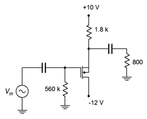
This follower uses a P-channel device with combination bias. Note that the source terminal is toward the top of the schematic. First, determine 𝑔𝑚0𝑅𝑆 and the bias factor, 𝑘 . Then the combination bias equation can be used to determine the drain current.
![\[g_{m0} =- \frac{2 \times 80 mA}{-2.5 V} \]](https://pressbooks.nscc.ca/app/uploads/quicklatex/quicklatex.com-852c21b67d9271b3f4e08f8e496c6039_l3.png "Rendered by QuickLaTeX.com")
![\[g_{m0} = 64 mS \]](https://pressbooks.nscc.ca/app/uploads/quicklatex/quicklatex.com-330f05472874eeba923472fcc429f95b_l3.png "Rendered by QuickLaTeX.com")
The DC source resistance is the 1.8 k Ω biasing resistor resulting in 𝑔𝑚0𝑅𝑆 = 115.2. The bias factor is 𝑉𝑆𝑆/𝑉𝐺𝑆(𝑜𝑓𝑓) , or 4. The combination bias equation (Equation 10.9) yields 𝐼𝐷 = 6.67 mA.
We can now find the transconductance and voltage gain.
![\[g_m = 64mS \sqrt{\frac{6.67 mA}{80mA}} \]](https://pressbooks.nscc.ca/app/uploads/quicklatex/quicklatex.com-dcefba478e00555f3702dd7845c99bbf_l3.png "Rendered by QuickLaTeX.com")
![\[g_m = 18.5mS \]](https://pressbooks.nscc.ca/app/uploads/quicklatex/quicklatex.com-e03495f2abc95596252bebdb6263cadc_l3.png "Rendered by QuickLaTeX.com")
The voltage gain is
![\[A_v = \frac{18.5 mS(1.8k \Omega || 800\Omega )}{18.5 mS \times (1.8 k\Omega || 800 \Omega ) +1} \]](https://pressbooks.nscc.ca/app/uploads/quicklatex/quicklatex.com-b7aa13ee54eaaaa24d9f4481425ac6a0_l3.png "Rendered by QuickLaTeX.com")
![\[A_v = 0.91 \]](https://pressbooks.nscc.ca/app/uploads/quicklatex/quicklatex.com-2b27c16657a3ab8a3e4d1ad3d2292fea_l3.png "Rendered by QuickLaTeX.com")
Lastly, the input impedance is
![\[Z_{in} = 560 k\Omega || Z_{in(gate)} \approx 560 k\Omega \]](https://pressbooks.nscc.ca/app/uploads/quicklatex/quicklatex.com-46858dad377ad488e08353621764286c_l3.png "Rendered by QuickLaTeX.com")
