
2.2 Simplified AC Model of the JFET
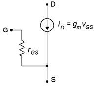
An AC model of the JFET is shown in Figure 11.2.1. This is essentially the same model as was used for DC analysis. Once again, we have a voltage-controlled current source situated in the drain. The reverse-biased junction shows up as a very large resistance, 𝑟𝐺𝑆.
It is worth mentioning that this model is suitable only for low frequencies. At higher frequencies, device capacitances can play a major role in the response of the amplifier. There are three device capacitances not shown in the Figure that shunt each pair of terminals: 𝐶𝐺𝑆, 𝐶𝐷𝐺 and 𝐶𝐷𝑆. On a data sheet, the “lumped” capacitances are often given. These are 𝐶𝑖𝑠𝑠, the capacitance looking into the gate with the source and drain shorted to ground: 𝐶𝑖𝑠𝑠=𝐶𝐺𝑆+𝐶𝐷𝐺; and 𝐶𝑟𝑠𝑠, the capacitance seen from the drain with the gate and source shorted to ground: 𝐶𝑟𝑠𝑠=𝐶𝐷𝑆+𝐶𝐷𝐺. As we shall see, these capacitances can have a sizable impact on amplifier characteristics such as 𝑍𝑖𝑛.
The value of transconductance, 𝑔𝑚, will prove to be of particular interest. It is roughly of equal importance to 𝑟′𝑒 in a BJT.[1]
- In fact, we can say that 1/𝑟′𝑒 is 𝑔𝑚 for a BJT. ↵
