
10.2 Inverting and Noninverting Amplifiers
As noted in our earlier work, negative feedback can be applied in one of four ways. The parallel input form inverts the input signal, and the series input form doesn’t. Because these forms were presented as current-sensing and voltage-sensing respectively, you might get the initial impression that all voltage amplifiers must be noninverting. This is not the case. With the simple inclusion of one or two resistors, for example, we can make inverting voltage amplifiers or noninverting current amplifiers. Virtually all topologies are realizable. We will look at the controlledvoltage source forms first (those using SP and PP negative feedback).
For analysis, you can use the classic treatment given in Chapter Three; however, due to some rather nice characteristics of the typical op amp, approximations will be shown. These approximations are only valid in the midband and say nothing of the high frequency performance of the circuit. Therefore, they are not suitable for general-purpose discrete work. The idealizations for the approximations are:
- The input current is virtually zero (i.e., 𝑍𝑖𝑛 is infinite).
- The potential difference between the inverting and noninverting inputs is virtually zero (i.e., loop gain is infinite). This signal is also called the error signal.
Also, note for clarity that the power supply connections are not shown in most of the diagrams.
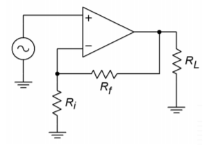
The Noninverting Voltage Amplifier
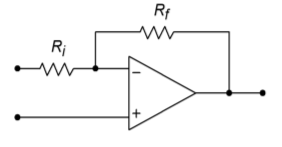
The noninverting voltage amplifier is based on SP negative feedback. An example is given in Figure 4.2.1 . Note the similarity to the generic SP circuits of Chapter Three. Recalling the basic action of SP negative feedback, we expect a very high 𝑍𝑖𝑛 , a very low 𝑍𝑜𝑢𝑡 , and a reduction in voltage gain. Idealization 1 states that 𝑍𝑖𝑛 must be infinite. We already know that op amps have low 𝑍𝑜𝑢𝑡 , the second item is taken care of. Now let’s take a look at voltage gain.
![\[A_{v} = \frac{V_{out}}{V_{in}} \]](https://pressbooks.nscc.ca/app/uploads/quicklatex/quicklatex.com-80f76025529af5ecc6775c93a20ab775_l3.png "Rendered by QuickLaTeX.com")
Because ideally 𝑉𝑒𝑟𝑟𝑜𝑟=0
![\[V_{in} = V_{Ri} \]](https://pressbooks.nscc.ca/app/uploads/quicklatex/quicklatex.com-a639ba8d637fc2c7024b127a719ea989_l3.png "Rendered by QuickLaTeX.com")
Also,
![\[V_{out} = V_{Ri} + V_{Rf} \]](https://pressbooks.nscc.ca/app/uploads/quicklatex/quicklatex.com-0a76c33d5c82d9f81a91c2b8b1538cc2_l3.png "Rendered by QuickLaTeX.com")
![\[A_v = \frac{V_{Ri} + V_{Rf}}{V_{Ri}} \]](https://pressbooks.nscc.ca/app/uploads/quicklatex/quicklatex.com-62f63a7ee2a8514678149c317eb7c131_l3.png "Rendered by QuickLaTeX.com")
Expansion gives
![\[A_v = \frac{R_i I_{Ri} + R_f I_{Rf}}{Ri I_{Ri}} \]](https://pressbooks.nscc.ca/app/uploads/quicklatex/quicklatex.com-d3315aba5e55b8db468cff45cef510c6_l3.png "Rendered by QuickLaTeX.com")
Because 𝐼𝑖𝑛=0 , 𝐼𝑅𝑓=𝐼𝑅𝑖 , and finally we come to
![\[A_v = \frac{R_i + R_f}{R_i} \text{or} \]](https://pressbooks.nscc.ca/app/uploads/quicklatex/quicklatex.com-d570912cc7cc759b053c055ad635b84d_l3.png "Rendered by QuickLaTeX.com")
![\[A_v = 1+ \frac{R_f}{R_i} \]](https://pressbooks.nscc.ca/app/uploads/quicklatex/quicklatex.com-3fead3440157629d6ec728f5898786be_l3.png "Rendered by QuickLaTeX.com")
(4.2.1)
Now that’s convenient. The gain of this amplifier is set by the ratio of two resistors. The larger 𝑅𝑓 is relative to 𝑅𝑖 , the more gain you get. Remember, this is an approximation. The closed loop gain can never exceed the open loop gain, and eventually, 𝐴𝑣 will fall off as frequency increases. Note that the calculation ignores the effect of the load impedance. Obviously, if 𝑅𝑙 is too small, the excessive current draw will cause the op amp to clip.
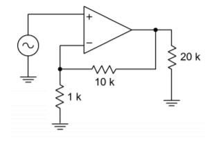
Example 4.2.1
What are the input impedance and gain of the circuit in Figure 4.2.2 ?
First off, 𝑍𝑖𝑛 is ideally infinite. Now for the gain:
![\[A_v = 1+ \frac{10 k}{1 k} \]](https://pressbooks.nscc.ca/app/uploads/quicklatex/quicklatex.com-7ce4556cce87cba23af02e219598cda8_l3.png "Rendered by QuickLaTeX.com")
![\[A_v = 11 \]](https://pressbooks.nscc.ca/app/uploads/quicklatex/quicklatex.com-6934256470cb1a104a99b7b5680596fb_l3.png "Rendered by QuickLaTeX.com")
The opposite process of amplifier design is just as straightforward.
Example 4.2.2
Design an amplifier with a gain of 26 dB and an input impedance of 47 k Ω . For the gain, first turn 26 dB into ordinary form. This is a voltage gain of about 20.
![\[\frac{R_f}{R_i} = A_v - 1 \]](https://pressbooks.nscc.ca/app/uploads/quicklatex/quicklatex.com-e97d7bb496367cfdff99b2af5c2c2291_l3.png "Rendered by QuickLaTeX.com")
![\[\frac{R_f}{R_i} = 19 \]](https://pressbooks.nscc.ca/app/uploads/quicklatex/quicklatex.com-c871a595ee65d2325fb7c26f076db845_l3.png "Rendered by QuickLaTeX.com")

At this point, choose a value for one of the resistors and solve for the other one. For example, the following would all be valid:
![\[R_i=1k \Omega ,\ R_f=19 k \Omega \]](https://pressbooks.nscc.ca/app/uploads/quicklatex/quicklatex.com-79ca550df389827da8a32438344e127f_l3.png "Rendered by QuickLaTeX.com")
![\[R_i=2 k \Omega ,\ R_f =38 k \Omega \]](https://pressbooks.nscc.ca/app/uploads/quicklatex/quicklatex.com-a8376495f459fe2ee638c078b61220ea_l3.png "Rendered by QuickLaTeX.com")
![\[R_i=500 \Omega ,\ R_f =9.5 k \Omega \]](https://pressbooks.nscc.ca/app/uploads/quicklatex/quicklatex.com-bdde29d36b1401d1e0a77c7b7fa1d491_l3.png "Rendered by QuickLaTeX.com")
Most of these are not standard values, though, and will need slight adjustments for a production circuit (see Appendix B). A reasonable range is 100𝑘Ω>𝑅𝑖+𝑅𝑓>10𝑘Ω . The accuracy of this gain will depend on the accuracy of the resistors. Now for the 𝑍𝑖𝑛 requirement. This is deceptively simple. 𝑍𝑖𝑛 is assumed to be infinite, so all you need to do is place a 47 k Ω in parallel with the input. The resulting circuit is shown in Figure 4.2.3 .
If a specific 𝑍𝑖𝑛 is not specified, a parallel input resistor is not required. There is one exception to this rule. If the driving source is not directly coupled to the op amp input (e.g., it is capacitively coupled), a resistor will be required to establish a DC return path to ground. Without a DC return path, the input section’s diff amp stage will not be properly biased. This point is worth remembering, as it can save you a great deal in future headaches. For example, in the lab a circuit like the one in Figure 4.2.2 may work fine with one function generator, but not with another. This would be the case if the second generator used an output coupling capacitor and the first one didn’t.
Example 4.2.3
Design a voltage follower (i.e., ideally infinite 𝑍𝑖𝑛 and a voltage gain of 1).
The 𝑍𝑖𝑛 part is straightforward enough. As for the second part, what ratio of 𝑅𝑓 to 𝑅𝑖 will yield a gain of 1?
![\[\frac{R_f}{R_i} = 0 \]](https://pressbooks.nscc.ca/app/uploads/quicklatex/quicklatex.com-eec37b4dd7a43b073397c616a899163a_l3.png "Rendered by QuickLaTeX.com")
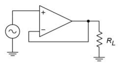
This says that 𝑅𝑓 must be 0 Ω . Practically speaking, that means that 𝑅𝑓 is replaced with a shorting wire. What about 𝑅𝑖 ? Theoretically, almost any value will do. As long as there’s a choice, consider infinite. Zero divided by infinite is certainly zero. The practical benefit of choosing 𝑅𝑖=∞ is that you may delete 𝑅𝑖 . The resulting circuit is shown in Figure 4.2.4 . Remember, if the source is not directly coupled, a DC return resistor will be needed. The value of this resistor has to be large enough to avoid loading the source.
As you can see, designing with op amps can be much quicker than its discrete counterpart. As a result, your efficiency as a designer or repair technician can improve greatly. You are now free to concentrate on the system, rather than on the specifics of an individual biasing resistor. In order to make multi-stage amplifiers, just link individual stages together.
Example 4.2.4
What is the input impedance of the circuit in Figure 4.2.5 ? What is 𝑉𝑜𝑢𝑡? As in any multi-stage amplifier, the input impedance to the first stage is the system 𝑍𝑖𝑛 . The DC return resistor sets this at 100 k Ω .

To find 𝑉𝑜𝑢𝑡, we need to find the gain (in dB).
![\[A_{v1} = 1+ \frac{R_f}{R_i} \]](https://pressbooks.nscc.ca/app/uploads/quicklatex/quicklatex.com-c0202177379af328684eacd5f2fcb344_l3.png "Rendered by QuickLaTeX.com")
![\[A_{v1} = 1+ \frac{14 k}{2 k} \]](https://pressbooks.nscc.ca/app/uploads/quicklatex/quicklatex.com-69805556508005850ec7b5cc7608276d_l3.png "Rendered by QuickLaTeX.com")
![\[A_{v1} = 8 \]](https://pressbooks.nscc.ca/app/uploads/quicklatex/quicklatex.com-faa9014bf17c277bb9267cfcfda771d6_l3.png "Rendered by QuickLaTeX.com")
![\[A_{v1}^{'} = 18 dB \]](https://pressbooks.nscc.ca/app/uploads/quicklatex/quicklatex.com-efb3c99f04ce6986237d6bd8a7e5d3c3_l3.png "Rendered by QuickLaTeX.com")
![\[A_{v2} = 1+ \frac{R_f}{R_i} \]](https://pressbooks.nscc.ca/app/uploads/quicklatex/quicklatex.com-bf6de4373af1c2af9eea11f2875ae26c_l3.png "Rendered by QuickLaTeX.com")
![\[A_{v2} = 1+ \frac{18 k}{2 k} \]](https://pressbooks.nscc.ca/app/uploads/quicklatex/quicklatex.com-0f4ab2327b7757a1f9c9eb3dd82f4947_l3.png "Rendered by QuickLaTeX.com")
![\[A_{v2} = 10 \]](https://pressbooks.nscc.ca/app/uploads/quicklatex/quicklatex.com-1f3a28bb9b10b0c2d1803e92b2e9f51f_l3.png "Rendered by QuickLaTeX.com")
![\[A_{v2}^{'} = 20 dB \]](https://pressbooks.nscc.ca/app/uploads/quicklatex/quicklatex.com-7b81ca205ea865b6696572a9bfde4618_l3.png "Rendered by QuickLaTeX.com")
![\[A_{vt}^{'} = 18 dB + 20 dB = 38 dB \]](https://pressbooks.nscc.ca/app/uploads/quicklatex/quicklatex.com-db8131e8dbd4c35fcfe04b53285ed2fd_l3.png "Rendered by QuickLaTeX.com")
![\[V_{out}^{'} = A_{vt}^{'} + V_{in}^{'} \]](https://pressbooks.nscc.ca/app/uploads/quicklatex/quicklatex.com-14b2b29f14263e2f5b2144ea1809ea6a_l3.png "Rendered by QuickLaTeX.com")
![\[V_{out}^{'} = 38 dB + (-30 dBV) \]](https://pressbooks.nscc.ca/app/uploads/quicklatex/quicklatex.com-500d26da4873966418854c2430069fd2_l3.png "Rendered by QuickLaTeX.com")
![\[V_{out}^{'} = 8 dBV \]](https://pressbooks.nscc.ca/app/uploads/quicklatex/quicklatex.com-885a7d17dac22574cc70d9d5e55939f3_l3.png "Rendered by QuickLaTeX.com")
Because 8 dBV translates to about 2.5 V, there is no danger of clipping either.
Inverting Voltage Amplifier
The inverting amplifier is based on the PP negative feedback model. The base form is shown in Figure 4.2.6 . By itself, this form is current sensing, not voltage sensing. In order to achieve voltage sensing, an input resistor, 𝑅𝑖 , is added. See Figure 4.2.7 . Here’s how the circuit works: 𝑉𝑒𝑟𝑟𝑜𝑟 is virtually zero, so the inverting input potential must equal the noninverting input potential. This means that the inverting input is at a virtual ground. The signal here is so small that it is negligible. Because of this, we may also say that the impedance seen looking into this point is zero. This last point may cause a bit of confusion. You may ask, “How can the impedance be zero if the current into the op amp is zero?” The answer lies in the fact that all of the entering current will be drawn through 𝑅𝑓 , thus bypassing the inverting input.

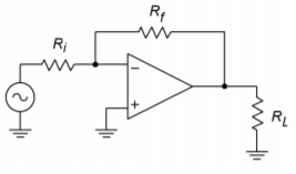
Refer to Figure 4.2.8 for the detailed explanation. The right end of 𝑅𝑖 is at virtual ground, so all of the input voltage drops across it, creating 𝐼𝑖𝑛 , the input current. This current cannot enter the op amp and instead will pass through 𝑅𝑓 . Because a positive signal is presented to the inverting input, the op amp will sink output current, thus drawing 𝐼𝑖𝑛 through 𝑅𝑓 . The resulting voltage drop across 𝑅𝑓 is the same magnitude as the load voltage. This is true because 𝑅𝑓 is effectively in parallel with the load. Note that both elements are tied to the op amp’s output and to (virtual) ground. There is a change in polarity because we reference the output signal to ground. In short, 𝑉𝑜𝑢𝑡is the voltage across 𝑅𝑓 , inverted.
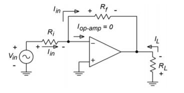
![\[A_v = \frac{V_{out}}{V_{in}} \]](https://pressbooks.nscc.ca/app/uploads/quicklatex/quicklatex.com-d77ecef6476113f154c9606d5e6f52af_l3.png "Rendered by QuickLaTeX.com")
![\[V_{in} = I_{in}R_i \]](https://pressbooks.nscc.ca/app/uploads/quicklatex/quicklatex.com-ae7e80e35eee0353acb52f727590e56f_l3.png "Rendered by QuickLaTeX.com")
![\[V_{out} = -V_{R_f} \]](https://pressbooks.nscc.ca/app/uploads/quicklatex/quicklatex.com-57d47aba13d6acf6669d7741f7d10df7_l3.png "Rendered by QuickLaTeX.com")
![\[V_{Rf} = I_{in} R_f \]](https://pressbooks.nscc.ca/app/uploads/quicklatex/quicklatex.com-f289bc1d74f1370bbe8ebf15c41bb67a_l3.png "Rendered by QuickLaTeX.com")
Substitution yields
![\[A_v = -\frac{I_{in}R_f}{I_{in}R_i} \]](https://pressbooks.nscc.ca/app/uploads/quicklatex/quicklatex.com-9a0be6c6783cb0052c44de00f95b2718_l3.png "Rendered by QuickLaTeX.com")
![\[A_v =- \frac{R_f}{R_i} \]](https://pressbooks.nscc.ca/app/uploads/quicklatex/quicklatex.com-b522303adfbb5804f5a0380296c5208b_l3.png "Rendered by QuickLaTeX.com")
(4.2.2)
Again, we see that the voltage gain is set by resistor ratio. Again, there is an allowable range of values.
The foregoing discussion points up the derivation of input impedance. Because all of the input signal drops across 𝑅𝑖 , it follows that all the driving source “sees” is 𝑅𝑖 . Quite simply, 𝑅𝑖 sets the input impedance. Unlike the noninverting voltage amp, there is a definite interrelation between 𝑍𝑖𝑛(𝑅𝑖) and 𝐴𝑣(−𝑅𝑓/𝑅𝑖) . This indicates that it is very hard to achieve both high gain and high 𝑍𝑖𝑛 with this circuit.
Example 4.2.5
Determine the input impedance and output voltage for the circuit in Figure 4.2.9 .

The input impedance is set by 𝑅𝑖 . 𝑅𝑖=5𝑘Ω , therefore 𝑍𝑖𝑛=5𝑘Ω .
![\[V_{out} = V_{in}A_v \]](https://pressbooks.nscc.ca/app/uploads/quicklatex/quicklatex.com-adbdeaab39c85a17f541e9c42f66e39b_l3.png "Rendered by QuickLaTeX.com")
![\[A_v = -\frac{R_f}{R_i} \]](https://pressbooks.nscc.ca/app/uploads/quicklatex/quicklatex.com-e22ad7fa5885e7aee6ff3c18a59aed2c_l3.png "Rendered by QuickLaTeX.com")
![\[A_v =-\frac{20 k}{5 k} \]](https://pressbooks.nscc.ca/app/uploads/quicklatex/quicklatex.com-459ff10c7bb8f8723d11e048e2ed3c21_l3.png "Rendered by QuickLaTeX.com")
![\[A_v =-4 \]](https://pressbooks.nscc.ca/app/uploads/quicklatex/quicklatex.com-aa6ff4388a6f0b7ae231a2c510d1de31_l3.png "Rendered by QuickLaTeX.com")
![\[V_{out} =100mV\times (-4) \]](https://pressbooks.nscc.ca/app/uploads/quicklatex/quicklatex.com-e4937b2cbe6d8e0f682a0d3c92298c4d_l3.png "Rendered by QuickLaTeX.com")
![\[V_{out} =-400 mV, \text{ (i.e., inverted)} \]](https://pressbooks.nscc.ca/app/uploads/quicklatex/quicklatex.com-4df7621bc488f59a0b48ae7ce0b9f7c8_l3.png "Rendered by QuickLaTeX.com")
Example 4.2.6
Design an inverting amplifier with a gain of 10 and an input impedance of 15 k Ω . The input impedance tells us what 𝑅𝑖 must be
![\[Z_{in} = R_i \]](https://pressbooks.nscc.ca/app/uploads/quicklatex/quicklatex.com-ab5f6b859985017c8e0589cafbe683a8_l3.png "Rendered by QuickLaTeX.com")
![\[R_i = 15 k \]](https://pressbooks.nscc.ca/app/uploads/quicklatex/quicklatex.com-8c383bffbf3ee08359cd504888a26470_l3.png "Rendered by QuickLaTeX.com")
Knowing 𝑅𝑖 , solve for 𝑅𝑓 :
![\[R_f =R_i(-A_v ) \]](https://pressbooks.nscc.ca/app/uploads/quicklatex/quicklatex.com-34fab59ac3e5c2eec21fb9718b273b5b_l3.png "Rendered by QuickLaTeX.com")
![\[R_f =15k\times (-(-10)) \]](https://pressbooks.nscc.ca/app/uploads/quicklatex/quicklatex.com-5e61d58933f392751640206aab165824_l3.png "Rendered by QuickLaTeX.com")
![\[R_f =150 k \]](https://pressbooks.nscc.ca/app/uploads/quicklatex/quicklatex.com-8c5818ae4f1f141ec8a5543265adb262_l3.png "Rendered by QuickLaTeX.com")
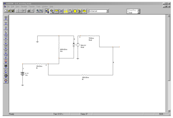
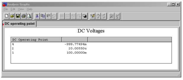
Computer Simulation
A Multisim simulation of the result of Example 4.2.6 is shown in Figure 4.2.10 , along with its schematic. This simulation uses the simple dependent source model presented in Chapter Two. The input is set at 0.1V DC for simplicity. Note that the output potential is negative, indicating the inverting action of the amplifier. Also, note that the virtual ground approximation is borne out quite well, with the inverting input potential measuring in the 𝜇 V region.
Example 4.2.7
The circuit of Figure 4.2.11 is a pre-amplifier stage for an electronic music keyboard. Like most musicians’ pre-amplifiers, this one offers adjustable gain. This is achieved by following the amplifier with a pot. What are the maximum and minimum gain values?
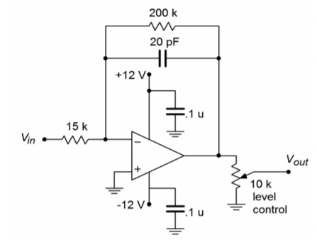
Note that the gain for the pre-amp is the product of the op amp gain and the voltage divider ratio produced by the pot. For maximum gain, use the pot in its uppermost position. Because the pot acts as a voltage divider, the uppermost position provides no divider action (i.e., its gain is unity). For midband frequencies, the 20 pF may be ignored.
![\[A_{v-max} =- \frac{R_f}{R_i} \]](https://pressbooks.nscc.ca/app/uploads/quicklatex/quicklatex.com-b54a37d1852470346b705e0093b39b6a_l3.png "Rendered by QuickLaTeX.com")
![\[A_{v-max} =- \frac{200 k}{15k} \]](https://pressbooks.nscc.ca/app/uploads/quicklatex/quicklatex.com-20ed0d74e7ff26735724f866ee47fa34_l3.png "Rendered by QuickLaTeX.com")
![\[A_{v-max} =- 13.33 \]](https://pressbooks.nscc.ca/app/uploads/quicklatex/quicklatex.com-5644bca89f4e7ab6fb10628aea5b9bf4_l3.png "Rendered by QuickLaTeX.com")
![\[A_{v-max}^{'} = 22.5 dB \]](https://pressbooks.nscc.ca/app/uploads/quicklatex/quicklatex.com-0c60f6eb3fe7da406076661219455717_l3.png "Rendered by QuickLaTeX.com")
For minimum gain, the pot is dialed to ground. At this point, the divider action is infinite, and thus the minimum gain is 0 (resulting in silence).
𝑍𝑖𝑛 for the system is about 15 k Ω . As far as the extra components are concerned, the 20 pF capacitor is used to decrease high frequency gain. The two 0.1 𝜇 F bypass capacitors across the power supply lines are very important. Virtually all op amp circuits use bypass capacitors. Due to the high gain nature of op amps, it is essential to have good AC grounds at the power supply pins. At higher frequencies the inductance of power supply wiring may produce a sizable impedance. This impedance may create a positive feedback loop that wouldn’t exist otherwise. Without the bypass capacitors, the circuit may oscillate or produce spurious output signals. The precise values for the capacitors are usually not critical, with 0.1 to 1 𝜇 F being typical.
Inverting Current-to-Voltage Transducer
As previously mentioned, the inverting voltage amplifier is based on PP negative feedback, with an extra input resistor used to turn the input voltage into a current. What happens if that extra resistor is left out, and a circuit such as Figure 4.2.6 is used? Without the extra resistor, the input is at virtual ground, thus setting 𝑍𝑖𝑛 to 0 Ω . This is ideal for sensing current. This input current will pass through 𝑅𝑓 and produce an output voltage as outlined above. The characteristic of transforming a current to a voltage is measured by the parameter transresistance. By definition, the transresistance of this circuit is the value of 𝑅𝑓 . To find 𝑉𝑜𝑢𝑡, multiply the input current by the transresistance. This circuit inverts polarity as well.
![\[V_{out} =−I_{in}R_f \]](https://pressbooks.nscc.ca/app/uploads/quicklatex/quicklatex.com-a1f2c301ca837fcf9c94470d49752adc_l3.png "Rendered by QuickLaTeX.com")
(4.2.3)
Example 4.2.8
Design a circuit based on Figure 4.2.6 if an input current of -50 𝜇 A should produce an output of 4 V.
The transresistance of the circuit is 𝑅𝑓
![\[R_f =- \frac{V_{out}}{I_{in}} \]](https://pressbooks.nscc.ca/app/uploads/quicklatex/quicklatex.com-63f2d7b42d076acfc89bf667ee13bc81_l3.png "Rendered by QuickLaTeX.com")
![\[R_f =- \frac{4 V}{−50\mu A} \]](https://pressbooks.nscc.ca/app/uploads/quicklatex/quicklatex.com-52391a49e66a8c630dc25c556c4ca353_l3.png "Rendered by QuickLaTeX.com")
![\[R_f = 80 k \]](https://pressbooks.nscc.ca/app/uploads/quicklatex/quicklatex.com-0aa90b7b2aa7a38d4d9516efd31506c8_l3.png "Rendered by QuickLaTeX.com")
The input impedance is assumed to be zero.
At first glance, the circuit applications of the topology presented in the prior example seem very limited. In reality, there are a number of linear integrated circuits that produce their output in current form.[1] In many cases, this signal must be turned into a voltage in order to properly interface with other circuit elements. The current-to-voltage transducer is widely used for this purpose.
Noninverting Voltage-to-Current Transducer
This circuit topology utilizes SS negative feedback. It senses an input voltage and produces a current. A conceptual comparison can be made to the FET (a voltage controlled current source). Instead of circuit gain, we are interested in transconductance. In other words, how much input voltage is required to produce a given output current? The op amp circuit presented here drives a floating load. That is, the load is not referenced to ground. This can be convenient in some cases, and a real pain in others. With some added circuitry, it is possible to produce a grounded load version, although space precludes us from examining it here.
A typical voltage-to-current circuit is shown in Figure 4.2.12 . Because this uses series-input type feedback, we may immediately assume that 𝑍𝑖𝑛 is infinite. The voltage to current ratio is set by feedback resistor 𝑅𝑖 . As 𝑉𝑒𝑟𝑟𝑜𝑟 is assumed to be zero, all of 𝑉𝑖𝑛drops across 𝑅𝑖 , creating current 𝐼𝑅𝑖 . The op amp is assumed to have zero input current, so all of 𝐼𝑅𝑖 flows through the load resistor, 𝑅𝑙 . By adjusting 𝑅𝑖 , the load current may be varied.
![\[I_{load} = I_{R_i} \]](https://pressbooks.nscc.ca/app/uploads/quicklatex/quicklatex.com-efff5e8f0fd0dbe7d3aee7b3d0a6bde6_l3.png "Rendered by QuickLaTeX.com")
![\[I_{R_i} = \frac{V_{in}}{R_i} \]](https://pressbooks.nscc.ca/app/uploads/quicklatex/quicklatex.com-a9b3d346da1adc72e913cc72270f68ed_l3.png "Rendered by QuickLaTeX.com")
![\[I_{load} = \frac{V_{in}}{R_i} \]](https://pressbooks.nscc.ca/app/uploads/quicklatex/quicklatex.com-04615c84c22222a440bbef477fb13294_l3.png "Rendered by QuickLaTeX.com")
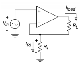
By definition,
![\[g_m = \frac{I_{load}}{V_{in}} \]](https://pressbooks.nscc.ca/app/uploads/quicklatex/quicklatex.com-2e17e84b32b9263d2c53fb2b57eb4fc5_l3.png "Rendered by QuickLaTeX.com")
![\[g_m = \frac{1}{R_i} \]](https://pressbooks.nscc.ca/app/uploads/quicklatex/quicklatex.com-225239699d7d93078df9f5199b5e5737_l3.png "Rendered by QuickLaTeX.com")
(4.2.4)
So, the transconductance of the circuit is set by the feedback resistor. As usual, there are practical limits to the size of 𝑅𝑖 . If 𝑅𝑖 and 𝑅𝑙 are too small, the possibility exists that the op amp will “run out” of output current and go into saturation. At the other extreme, the product of the two resistors and the 𝐼𝑙𝑜𝑎𝑑 cannot exceed the power supply rails. As an example, if 𝑅𝑖 plus 𝑅𝑙 is 10 k Ω , 𝐼𝑙𝑜𝑎𝑑 cannot exceed about 1.5 mA if standard ± 15 V supplies are used.
Example 4.2.9
Given an input voltage of 0.4 V in the circuit of Figure 4.2.13 , what is the load current?
![\[g_m = \frac{1}{20 k} \]](https://pressbooks.nscc.ca/app/uploads/quicklatex/quicklatex.com-67a432abe0ab4abc44241508993a2922_l3.png "Rendered by QuickLaTeX.com")
![\[g_m = 50 \mu S \]](https://pressbooks.nscc.ca/app/uploads/quicklatex/quicklatex.com-2a411c59e23f3c85d1df0746108c6e7f_l3.png "Rendered by QuickLaTeX.com")
![\[I_{load} = g_m V_{in} \]](https://pressbooks.nscc.ca/app/uploads/quicklatex/quicklatex.com-72c3132d4e2a40e4ed3bcc48117cd65d_l3.png "Rendered by QuickLaTeX.com")
![\[I_{load} = 50 \mu S\times 0.4 V \]](https://pressbooks.nscc.ca/app/uploads/quicklatex/quicklatex.com-95eb52ea5304c91f577facbeed300305_l3.png "Rendered by QuickLaTeX.com")
![\[I_{load} = 20 \mu A \]](https://pressbooks.nscc.ca/app/uploads/quicklatex/quicklatex.com-af9c31529c6540cee2fa43c940d8bc19_l3.png "Rendered by QuickLaTeX.com")
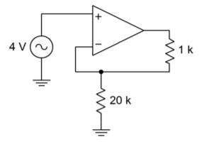
There is no danger of current overload here as the average op amp can produce about 20 mA, maximum. The output current will be 20 𝜇 A regardless of the value of 𝑅𝑙 , up to clipping. There is no danger of clipping in this situation either. The voltage seen at the output of the op amp to ground is
![\[V_{max} = (R_i+ R_l) I_{load} \]](https://pressbooks.nscc.ca/app/uploads/quicklatex/quicklatex.com-b15ffacd69a9f7354b922da9c40f69a7_l3.png "Rendered by QuickLaTeX.com")
![\[V_{max} = (20 k+1k)\times 20 \mu A \]](https://pressbooks.nscc.ca/app/uploads/quicklatex/quicklatex.com-68bfbd3cf7855dc6dbb2a042ef2ca3ce_l3.png "Rendered by QuickLaTeX.com")
![\[V_{max} = 420 mV \]](https://pressbooks.nscc.ca/app/uploads/quicklatex/quicklatex.com-308eea9f23c4170b175ea54eab75717d_l3.png "Rendered by QuickLaTeX.com")
That’s well below clipping level.
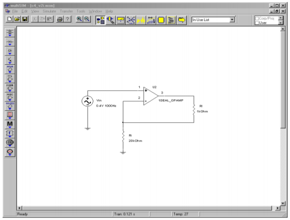
Computer Simulation
A simulation of the circuit of Example 4.2.9 is shown in Figure 4.2.14 . Multisim’s ideal op amp model has been chosen to simplify the layout. The load current is exactly as calculated at 20 𝜇 A. An interesting trick is used here to plot the load current, as many simulators only offer plotting of node voltages. Using Multisim’s Post Processor, the load current is computed by taking the difference between the node voltages on either side of the load resistor and then dividing the result by the load resistance.

Example 4.2.10
The circuit of Figure 4.2.15 can be used to make a high-input-impedance DC voltmeter. The load in this case is a simple meter movement. This particular meter requires 100 𝜇 A for full-scale deflection. If we want to measure voltages up to 10 V, what must 𝑅𝑖 be?
First, we must find the transconductance.
![\[g_m = \frac{100 \mu A}{10 V} \]](https://pressbooks.nscc.ca/app/uploads/quicklatex/quicklatex.com-75903df9704994c3f10ab75bb5de87b0_l3.png "Rendered by QuickLaTeX.com")
![\[g_m = 10 \mu S \]](https://pressbooks.nscc.ca/app/uploads/quicklatex/quicklatex.com-37b2f04c070064ac50059012902f14c1_l3.png "Rendered by QuickLaTeX.com")
![\[R_i = \frac{1}{g_m} \]](https://pressbooks.nscc.ca/app/uploads/quicklatex/quicklatex.com-46499a1e86a24b1eaf4e36c4f8ea91ef_l3.png "Rendered by QuickLaTeX.com")
![\[R_i = \frac{1}{10 \mu S} \]](https://pressbooks.nscc.ca/app/uploads/quicklatex/quicklatex.com-75c24598adb22c06152d3a23d81e72b5_l3.png "Rendered by QuickLaTeX.com")
![\[R_i =100 k \]](https://pressbooks.nscc.ca/app/uploads/quicklatex/quicklatex.com-15949e282a5ea626e8236e1b05c0404b_l3.png "Rendered by QuickLaTeX.com")
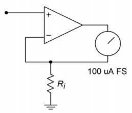
The meter deflection is assumed to be linear. For example, if the input signal is only 5 V, the current produced is halved to 50 𝜇 A. 50 𝜇 A should produce half-scale deflection. The accuracy of this electronic voltmeter depends on the accuracy of 𝑅𝑖 , and the linearity of the meter movement. Note that this little circuit can be quite convenient in a lab, being powered by batteries. In order to change scales, new values of 𝑅𝑖 can be swapped in with a rotary switch. For a 1 V scale, 𝑅𝑖 equals 10 k Ω . Note that for higher input ranges, some form of input attenuator is needed. This is due to the fact that most op amps may be damaged if input signals larger than the supply rails are used.
Inverting Current Amplifier
The inverting current amplifier uses PS negative feedback. As in the voltage-to-current transducer, the load is floating. The basic circuit is shown in Figure 4.2.16 . Due to the parallel negative feedback connection at the input, the circuit input impedance is assumed to be zero. This means that the input point is at virtual ground. The current into the op amp is negligible, so all input current flows through 𝑅𝑖 to node A. Effectively, 𝑅𝑖 and 𝑅𝑓 are in parallel (they both share node A and ground; actually virtual ground for 𝑅𝑖 ). Therefore, 𝑉𝑅𝑖 and 𝑉𝑅𝑓 are the same value. This means that a current is flowing through 𝑅𝑓 , from ground to node A. These two currents join to form the load current. In this manner, current gain is achieved. The larger 𝐼𝑅𝑓 is relative to 𝐼𝑖𝑛 , the more current gain there is. As the op amp is sinking current, this is an inverting amplifier.

![\[A_i =- \frac{I_{out}}{I_{in}} \]](https://pressbooks.nscc.ca/app/uploads/quicklatex/quicklatex.com-5449ff26bbba1b99c11e1f68edcf9dcb_l3.png "Rendered by QuickLaTeX.com")
![\[I_{out} = I_{Rf} + I_{Ri} \]](https://pressbooks.nscc.ca/app/uploads/quicklatex/quicklatex.com-57743610b703535ddf3292987e030cc0_l3.png "Rendered by QuickLaTeX.com")
(4.2.5)
![\[I_{Ri} = I_{in} \]](https://pressbooks.nscc.ca/app/uploads/quicklatex/quicklatex.com-07a98523b924c5b1e29a20af20d9baf0_l3.png "Rendered by QuickLaTeX.com")
![\[I_{Rf} = \frac{V_{Rf}}{R_f} \]](https://pressbooks.nscc.ca/app/uploads/quicklatex/quicklatex.com-8fabea3059b41c8af18ff40274db600d_l3.png "Rendered by QuickLaTeX.com")
Because 𝑉𝑅𝑓 is the same value as 𝑉𝑅𝑖 ,
![\[I_{Rf} = \frac{V_{Ri}}{R_f} \]](https://pressbooks.nscc.ca/app/uploads/quicklatex/quicklatex.com-96bc479c32c2a9417344ccbd63b00f87_l3.png "Rendered by QuickLaTeX.com")
(4.2.6)
![\[V_{Ri} = I_{in} R_i \]](https://pressbooks.nscc.ca/app/uploads/quicklatex/quicklatex.com-44095152247f9a53140592c63579deed_l3.png "Rendered by QuickLaTeX.com")
(4.2.7)
Substitution of 4.2.7 into 4.2.6 yields
![\[I_{Rf} = \frac{I_{in}R_i}{R_f} \]](https://pressbooks.nscc.ca/app/uploads/quicklatex/quicklatex.com-ab65fbd21a85fa49e14c13debd9a33c2_l3.png "Rendered by QuickLaTeX.com")
Substituting into 4.2.5 produces
![\[I_{out} = I_{in} + \frac{I_{in}R_i}{R_f} \]](https://pressbooks.nscc.ca/app/uploads/quicklatex/quicklatex.com-6fcc487e8e0297ef73ec1deae159449a_l3.png "Rendered by QuickLaTeX.com")
![\[I_{out} = I_{in}\left(1+ \frac{R_i}{R_f}\right) \]](https://pressbooks.nscc.ca/app/uploads/quicklatex/quicklatex.com-66f614e4dcbbbd30d25178ab3df7f06e_l3.png "Rendered by QuickLaTeX.com")
![\[A_i = -\left(1+ \frac{R_i}{R_f}\right) \]](https://pressbooks.nscc.ca/app/uploads/quicklatex/quicklatex.com-5f79cbe94fd202338f11fdfa502028a2_l3.png "Rendered by QuickLaTeX.com")
(4.2.8)
As you might expect, the gain is a function of the two feedback resistors. Note the similarity of this result with that of the noninverting voltage amplifier.
Example 4.2.11
What is the load current in Figure 4.2.17 ?
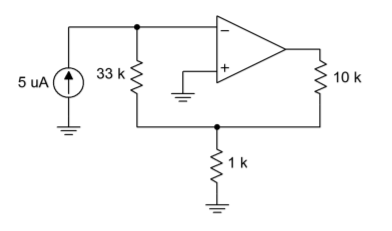
![\[I_{out} = -A_i I_{in} \]](https://pressbooks.nscc.ca/app/uploads/quicklatex/quicklatex.com-8e4197b163978641f95042795245758f_l3.png "Rendered by QuickLaTeX.com")
![\[A_i = -(1+ \frac{R_i}{R_f}) \]](https://pressbooks.nscc.ca/app/uploads/quicklatex/quicklatex.com-ccc9514e6ab5e578e3e6f0b1d5c68da2_l3.png "Rendered by QuickLaTeX.com")
![\[A_i = -(1+ \frac{33 k}{1 k}) \]](https://pressbooks.nscc.ca/app/uploads/quicklatex/quicklatex.com-70d7db7fa112a795404d07e3cd726646_l3.png "Rendered by QuickLaTeX.com")
![\[A_i = -34 \]](https://pressbooks.nscc.ca/app/uploads/quicklatex/quicklatex.com-1607264dce63648c739684fb812ec791_l3.png "Rendered by QuickLaTeX.com")
![\[I_{out} =-34\times 5 \mu A \]](https://pressbooks.nscc.ca/app/uploads/quicklatex/quicklatex.com-979aea069b77915d2f20e0ebdab487b2_l3.png "Rendered by QuickLaTeX.com")
![\[I_{out} =-170 \mu A \text{ (sinking)} \]](https://pressbooks.nscc.ca/app/uploads/quicklatex/quicklatex.com-2064a4d8fd8ded95a5c21b1851edc601_l3.png "Rendered by QuickLaTeX.com")
We need to check to make sure that this current doesn’t cause output clipping. A simple Ohm’s Law check is all that’s needed.
![\[V_{max} = I_{out} R_{load} +I_{in}R_i \]](https://pressbooks.nscc.ca/app/uploads/quicklatex/quicklatex.com-9d7f235af9756fddb3f67d807416ccf4_l3.png "Rendered by QuickLaTeX.com")
![\[V_{max} =170 \mu A\times 10 k+5 \mu A\times 33k \]](https://pressbooks.nscc.ca/app/uploads/quicklatex/quicklatex.com-f9e1b7b9c036b87e7d9def093dec3f36_l3.png "Rendered by QuickLaTeX.com")
![\[V_{max} = 1.7V+.165 V \]](https://pressbooks.nscc.ca/app/uploads/quicklatex/quicklatex.com-c4a42653bcee3dcb4dd48a98126387df_l3.png "Rendered by QuickLaTeX.com")
![\[V_{max} = 1.865V \text{ (no problem)} \]](https://pressbooks.nscc.ca/app/uploads/quicklatex/quicklatex.com-55e72beefe1460b571d2aa6737d5df44_l3.png "Rendered by QuickLaTeX.com")
Example 4.2.12
Design an amplifier with a current gain of -50. The load is approximately 200 k Ω . Assuming a typical op amp ( 𝐼𝑜𝑢𝑡−𝑚𝑎𝑥 = 20 mA with ± 15 V supplies), what is the maximum load current obtainable?
![\[A_i =-\left(1+ \frac{R_i}{R_f}\right) \]](https://pressbooks.nscc.ca/app/uploads/quicklatex/quicklatex.com-696d10a8511522ac345a85ffeeafb72c_l3.png "Rendered by QuickLaTeX.com")
![\[\frac{R_i}{R_f} =-Ai -1 \]](https://pressbooks.nscc.ca/app/uploads/quicklatex/quicklatex.com-974f0aa9d2df914a5226632314314d15_l3.png "Rendered by QuickLaTeX.com")
![\[\frac{R_i}{R_f} = 50-1 \]](https://pressbooks.nscc.ca/app/uploads/quicklatex/quicklatex.com-41c4b33d7b10215675def111ae39b39b_l3.png "Rendered by QuickLaTeX.com")
![\[\frac{R_i}{R_f} = 49 \]](https://pressbooks.nscc.ca/app/uploads/quicklatex/quicklatex.com-2a132aeed4e593be6bb71c4f0bbf44fc_l3.png "Rendered by QuickLaTeX.com")
Therefore, 𝑅𝑖 must be 49 times larger than 𝑅𝑓 . Possible solutions include:
![\[R_i = 49k \Omega , R_f = 1 k\Omega \]](https://pressbooks.nscc.ca/app/uploads/quicklatex/quicklatex.com-3f478b0efeb60c32f449e5c667ff63fc_l3.png "Rendered by QuickLaTeX.com")
![\[R_i = 98 k\Omega , R_f = 2 k\Omega \]](https://pressbooks.nscc.ca/app/uploads/quicklatex/quicklatex.com-02ca06f0296241e1fcb7821102c63cbc_l3.png "Rendered by QuickLaTeX.com")
![\[R_i = 24.5 k \Omega , R_f = 500\Omega \]](https://pressbooks.nscc.ca/app/uploads/quicklatex/quicklatex.com-625dad97fdd79723a5ede47e073f9a87_l3.png "Rendered by QuickLaTeX.com")
As far as maximum load current is concerned, it can be no greater than the op amp’s maximum output of 20 mA, but it may be less. We need to determine the current at clipping. Due to the large size of the load resistance, virtually all of the output potential will drop across it. Ignoring the extra drop across the feedback resistors will introduce a maximum of 1% error (that’s worst case, assuming resistor set number two).
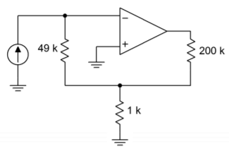
With 15 V rails, a typical op amp will clip at 13.5 V. The resulting current is found through Ohm’s Law:
![\[I_{max} = \frac{13.5 V}{200 k} \]](https://pressbooks.nscc.ca/app/uploads/quicklatex/quicklatex.com-2b0fe1f918063f003c16da21374c881a_l3.png "Rendered by QuickLaTeX.com")
![\[I_{max} = 67.5 \mu A \]](https://pressbooks.nscc.ca/app/uploads/quicklatex/quicklatex.com-534adcd23eeff38e9b2f1b783d6f8536_l3.png "Rendered by QuickLaTeX.com")
Another way of looking at this is to say that the maximum allowable input current is 67.5 𝜇 A/50, or 1.35 𝜇 A. One possible solution is shown in Figure 4.2.18 .
Summing Amplifiers
It is very common in circuit design to combine several signals into a single common signal. One good example of this is in the broadcast and recording industries. The typical modern music recording will require the use of perhaps dozens of microphones, yet the final product consists of typically two output signals (stereo left and right). If signals are joined haphazardly, excessive interference, noise, and distortion may result. The ideal summing amplifier would present each input signal with an isolated load not affected by other channels.
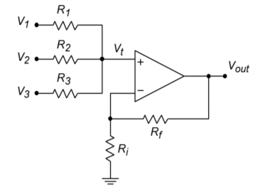
The most common form of summing amplifier is really nothing more than an extension of the inverting voltage amplifier. Because the input to the op amp is at virtual ground, it makes an ideal current summing node. Instead of placing a single input resistor at this point, several input resistors may be used. Each input source drives its own resistor, and there is very little affect from neighboring inputs. The virtual ground is the key. A general summing amplifier is shown in Figure 4.2.19 .
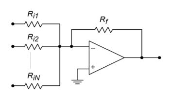
The input impedance for the first channel is 𝑅𝑖1 , and it’s voltage gain is −𝑅𝑓/𝑅𝑖1 . For channel 2, the input impedance is 𝑅𝑖2 , with a gain of −𝑅𝑓/𝑅𝑖2 . In general, then for channel N we have
![\[Z_{in N} = R_{i N} \]](https://pressbooks.nscc.ca/app/uploads/quicklatex/quicklatex.com-905d0a007d818e666f04018549aca647_l3.png "Rendered by QuickLaTeX.com")
![\[A_{v N} =- \frac{R_f}{R_{i N}} \]](https://pressbooks.nscc.ca/app/uploads/quicklatex/quicklatex.com-058fe8d7464dbe15d332fd6fd8af7a66_l3.png "Rendered by QuickLaTeX.com")
The output signal is the sum of all inputs multiplied by their associated gains.
![\[V_{out} = V_{in1} A_{v1} + V_{in2} A_{v2} + \dots + V_{in N} A_{v N} \]](https://pressbooks.nscc.ca/app/uploads/quicklatex/quicklatex.com-30727ca54b5684c24f9edadc2c26c54c_l3.png "Rendered by QuickLaTeX.com")
which is written more conveniently as
![\[V_{out} = \sum_{i=1}^{n}{V_{in_i} A_{v_i}} \]](https://pressbooks.nscc.ca/app/uploads/quicklatex/quicklatex.com-0df7f546eb6a293361ead724a4cde3f2_l3.png "Rendered by QuickLaTeX.com")
(4.2.9)
A summing amplifier may have equal gain for each input channel. This is referred to as an equal-weighted configuration.
Example 4.2.13
What is the output of the summing amplifier in Figure 4.2.20 , with the given DC input voltages?
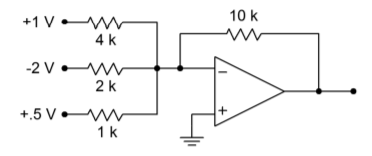
The easy way to approach this is to just treat the circuit as three inverting voltage amplifiers, and then add the results to get the final output.
Channel 1:
![\[A_v = - \frac{R_f}{R_i} \]](https://pressbooks.nscc.ca/app/uploads/quicklatex/quicklatex.com-52c113ae0e160b6daf3b62a265a4795f_l3.png "Rendered by QuickLaTeX.com")
![\[A_v = - \frac{10 k}{4 k} \]](https://pressbooks.nscc.ca/app/uploads/quicklatex/quicklatex.com-3fdd208943b7e3d5beaac6843eaa4e3a_l3.png "Rendered by QuickLaTeX.com")
![\[A_v = -2.5 \]](https://pressbooks.nscc.ca/app/uploads/quicklatex/quicklatex.com-bd877c2bf420ab95ccd9ffc72e529152_l3.png "Rendered by QuickLaTeX.com")
![\[V_{out} = -2.5\times 1V \]](https://pressbooks.nscc.ca/app/uploads/quicklatex/quicklatex.com-56eeb88ebd552801c7f4e4895d37680a_l3.png "Rendered by QuickLaTeX.com")
![\[V_{out} = -2.5 V \]](https://pressbooks.nscc.ca/app/uploads/quicklatex/quicklatex.com-a2ecc9f8bb0b50cf2631ac20cb7955df_l3.png "Rendered by QuickLaTeX.com")
Channel 2:
![\[A_v = - \frac{10 k}{2 k} \]](https://pressbooks.nscc.ca/app/uploads/quicklatex/quicklatex.com-ab29c6096b19f35cf2c0f1799584fa5b_l3.png "Rendered by QuickLaTeX.com")
![\[A_v = -5 \]](https://pressbooks.nscc.ca/app/uploads/quicklatex/quicklatex.com-6daedf01e1fa376096fd91874a02e159_l3.png "Rendered by QuickLaTeX.com")
![\[V_{out} = -5\times -2 V \]](https://pressbooks.nscc.ca/app/uploads/quicklatex/quicklatex.com-b62a8ba22ec0e5b737cd8beb4157b514_l3.png "Rendered by QuickLaTeX.com")
![\[V_{out} = 10 V \]](https://pressbooks.nscc.ca/app/uploads/quicklatex/quicklatex.com-374bbd318970f00e3cee5142643ea4b1_l3.png "Rendered by QuickLaTeX.com")
Channel 3:
![\[A_v = - \frac{10 k}{1 k} \]](https://pressbooks.nscc.ca/app/uploads/quicklatex/quicklatex.com-f4ffa1afe1bb6803b46ee72ddc8c1de7_l3.png "Rendered by QuickLaTeX.com")
![\[A_v = -10 \]](https://pressbooks.nscc.ca/app/uploads/quicklatex/quicklatex.com-532519254d762a7c44a56071341d583a_l3.png "Rendered by QuickLaTeX.com")
![\[V_{out} = -10\times .5 V \]](https://pressbooks.nscc.ca/app/uploads/quicklatex/quicklatex.com-03934741d2746b89d62ab51cd84699c4_l3.png "Rendered by QuickLaTeX.com")
![\[V_{out} = -5 V \]](https://pressbooks.nscc.ca/app/uploads/quicklatex/quicklatex.com-7fb77790e97e41418df7b5ea021b903b_l3.png "Rendered by QuickLaTeX.com")
The final output is found via summation:
![\[V_{out} =-2.5 V+10 V+(-5 V) \]](https://pressbooks.nscc.ca/app/uploads/quicklatex/quicklatex.com-a113b5c2b895d4b0d9ae7b391184a694_l3.png "Rendered by QuickLaTeX.com")
![\[V_{out} = 2.5 V \]](https://pressbooks.nscc.ca/app/uploads/quicklatex/quicklatex.com-e965747772a618f8248650395c610ec0_l3.png "Rendered by QuickLaTeX.com")
If the inputs were AC signals, the summation is not quite so straightforward. Remember, AC signals of differing frequency and phase do not add coherently. You can perform a calculation similar to the preceding to find the peak value, however, an RMS calculation is needed for the effective value (i.e., square root of the sum of the squares).
For use in the broadcast and recording industries, summing amplifiers will also require some form of volume control for each input channel and a master volume control as well. This allows the levels of various microphones or instruments to be properly balanced. Theoretically, individual-channel gain control may be produced by replacing each input resistor with a potentiometer. By adjusting 𝑅𝑖 , the gain may be directly varied. In practice, there are a few problems with this arrangement. First of all, it is impossible to turn a channel completely off. The required value for 𝑅𝑖 would be infinite. Second, because 𝑅𝑖 sets the input impedance, a variation in gain will produce a 𝑍𝑖𝑛 change. This change may overload or alter the characteristics of the driving source. One possible solution is to keep 𝑅𝑖 at a fixed value and place a potentiometer before it, as in Figure 4.2.21 . The pot produces a gain from 1 through 0. The 𝑅𝑓/𝑅𝑖 combo is then set for maximum gain. As long as 𝑅𝑖 is several times larger than the pot’s value, the channel’s input impedance will stay relatively constant. The effective 𝑍𝑖𝑛 for the channel is 𝑅𝑝𝑜𝑡 in parallel with 𝑅𝑖 , at a minimum, up to 𝑅𝑝𝑜𝑡 .
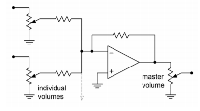
As far as a master volume control is concerned, it is possible to use a pot for 𝑅𝑓 . Without a limiting resistor though, a very low master gain runs the risk of over driving the op amp due to the small effective 𝑅𝑓 value. This technique also causes variations in offset potentials and circuit bandwidth. A technique that achieves higher performance involves using a stage with a fixed 𝑅𝑓 value, followed with a pot, as in Figure 4.2.21 .
Still another application of the summing amplifier is the level shifter. A level shifter is a two-input summing amplifier. One input is the desired AC signal, and the second input is a DC value. The proper selection of DC value lets you place the AC signal at a desired DC offset. There are many uses for such a circuit. One possible application is the DC offset control available on many signal generators.
Noninverting Summing Amplifier
Besides the inverting form, summing amplifiers may also be produced in a noninverting form. Noninverting summers generally exhibit superior high frequency performance when compared to the inverting type. One possible circuit is shown in Figure 4.2.22 . In this example, three inputs are shown, although more could be added. Each input has an associated input resistor. Note that it is not possible to simply wire several sources together in hopes of summing their respective signals. This is because each source will try to bring its output to a desired value that will be different from the values created by the other sources. The resulting imbalance may cause excessive (and possibly damaging) source currents. Consequently, each source must be isolated from the others through a resistor.
In order to understand the operation of this circuit it is best to break it into two parts: the input source/resistor section and the noninverting amplifier section. The input signals will combine to create a total input voltage, 𝑉𝑡 . By inspection, you should see that the output voltage of the circuit will equal 𝑉𝑡 times the noninverting gain, or
![\[V_{out} = V_t \left( 1+ \frac{R_f}{R_i} \right) \]](https://pressbooks.nscc.ca/app/uploads/quicklatex/quicklatex.com-d6dc30bf8833378e4b12af13563235d1_l3.png "Rendered by QuickLaTeX.com")
All that remains is to determine 𝑉𝑡 . Each of the input channels contributes to 𝑉𝑡 in a similar manner, so the derivation of the contribution from a single channel will be sufficient.
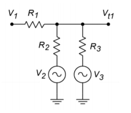
Unlike the inverting summer, the noninverting summer does not take advantage of the virtual-ground summing node. The result is that individual channels will affect each other. The equivalent circuit for channel 1 is redrawn in Figure 4.2.23 . Using superposition, we would first replace the input generators of channels 2 and 3 with short circuits. The result is a simple voltage divider between 𝑉1 and 𝑉𝑡1 .
![\[V_{t 1} = V_1 \frac{R_2 || R_3}{R_1 + R_2 || R_3} \]](https://pressbooks.nscc.ca/app/uploads/quicklatex/quicklatex.com-a8a8d5003287516f6117d786fb22640c_l3.png "Rendered by QuickLaTeX.com")
In a similar manner, we can derive the portions of 𝑉𝑡 due to channel 2
![\[V_{t 2} = V_2 \frac{R_1 || R_3}{R_2 + R_1 || R_3} \]](https://pressbooks.nscc.ca/app/uploads/quicklatex/quicklatex.com-b0bf6781b623e03187bdb113a17ecbfd_l3.png "Rendered by QuickLaTeX.com")
and due to channel 3
![\[V_{t 3} = V_3 \frac{R_1 || R_2}{R_3 + R_1 || R_2} \]](https://pressbooks.nscc.ca/app/uploads/quicklatex/quicklatex.com-22cf876b089050dac4b9274d191078d3_l3.png "Rendered by QuickLaTeX.com")
𝑉𝑡 is the summation of these three portions.
![\[V_t = V_{t 1} + V_{t 2} + V_{t 3} \]](https://pressbooks.nscc.ca/app/uploads/quicklatex/quicklatex.com-1a2899e895a357b6e40ebd29b4dc595c_l3.png "Rendered by QuickLaTeX.com")
Thus, by combining these elements, we find that the output voltage is
![\[V_{out} = \left( 1+ \frac{R_f}{R_i} \right) \left( V_1 \frac{R_2 || R_3}{R_1 + R_2 || R_3} + V_2 \frac{R_1 || R_3}{R_2 + R_1 || R_3} + V_3 \frac{R_1 || R_2}{R_3 + R_1 || R_2} \right) \]](https://pressbooks.nscc.ca/app/uploads/quicklatex/quicklatex.com-df61514a845c282ff34e7a2ac0be20ea_l3.png "Rendered by QuickLaTeX.com")
For convenience and equal weighting, the input resistors are often all set to the same value. This results in a circuit that averages together all of the inputs. Doing so simplifies the Equation to
![\[V_{out} = \left( 1+ \frac{R_f}{R_i} \right) \frac{V_1+V_2+V_3}{3} \]](https://pressbooks.nscc.ca/app/uploads/quicklatex/quicklatex.com-a49ce070b47f07e4b84ba81fb134db52_l3.png "Rendered by QuickLaTeX.com")
or in a more general sense,
![\[V_{out} = \left( 1+ \frac{R_f}{R_i} \right) \frac{\sum_{i=1}^{n}{V_n}}{n} \]](https://pressbooks.nscc.ca/app/uploads/quicklatex/quicklatex.com-11a1dc624bc93dfd836f7b27c7506833_l3.png "Rendered by QuickLaTeX.com")
(4.2.10)
where 𝑛 is the number of channels.
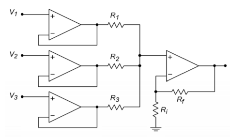
One problem still remains with this circuit, and that is inter-channel isolation or crosstalk. This can be eliminated by individually buffering each input, as shown in Figure 4.2.24 .
Example 4.2.14
A noninverting summer such as the one shown in Figure 4.2.22 is used to combine three signals. 𝑉1 = 1 V DC, 𝑉2 = -0.2 V DC, and 𝑉3 is a 2 V peak 100 Hz sine wave. Determine the output voltage if 𝑅1=𝑅2=𝑅3=𝑅𝑓 = 20 k Ω and 𝑅𝑖 = 5 k Ω .
Because all of the input resistors are equal, we can use the general form of the summing equation.
![\[V_{out} = \left( 1+ \frac{R_f}{R_i} \right) \frac{V_1+V_2+\dpts+V_n}{\text{Number of channels}} \]](https://pressbooks.nscc.ca/app/uploads/quicklatex/quicklatex.com-2618e1ade7caaa404ea82436697eb29b_l3.png "Rendered by QuickLaTeX.com")
![\[V_{out} = \left( 1+ \frac{20 k}{5 k} \right) \frac{1 VDC+(-0.2 VDC)+2 \sin2 \pi 100 t}{3} \]](https://pressbooks.nscc.ca/app/uploads/quicklatex/quicklatex.com-c68b65c4366a500b54642b9f3f33bfbf_l3.png "Rendered by QuickLaTeX.com")
![\[V_{out} = 5 \frac{0.8 VDC+2 \sin2 \pi 100 t}{3} \]](https://pressbooks.nscc.ca/app/uploads/quicklatex/quicklatex.com-80affa949e3fa37c87fc8595c3b2b4c8_l3.png "Rendered by QuickLaTeX.com")
![\[V_{out} = 1.33 VDC+3.33 \sin2 \pi 100 t \]](https://pressbooks.nscc.ca/app/uploads/quicklatex/quicklatex.com-a087f89258eb1862934c6edc80d36fc8_l3.png "Rendered by QuickLaTeX.com")
So we see that the output is a 3.33 V peak sine wave riding on a 1.33 V DC offset.
Differential Amplifier
As long as the op amp is based on a differential input stage, there is nothing preventing you from making a diff amp with it. The applications of an op amp based unit are the same as the discrete version examined in Chapter One. In essence, the differential amplifier configuration is a combination of the inverting and noninverting voltage amplifiers. A candidate is seen in Figure 4.2.25 . The analysis is identical to that of the two base types, and Superposition is used to combine the results. The obvious problem for this circuit is that there is a large mismatch between the gains if lower values are used. Remember, for the inverting input the gain magnitude is 𝑅𝑓/𝑅𝑖 , whereas the noninverting input sees 𝑅𝑓/𝑅𝑖 + 1. For proper operation, the gains of the two halves should be identical. The noninverting input has a slightly higher gain, so a simple voltage divider may be used to compensate. This is shown in Figure 4.2.26 . The ratio should be the same as the 𝑅𝑓/𝑅𝑖 ratio. The target gain is 𝑅𝑓/𝑅𝑖 , the present gain is 1 + 𝑅𝑓/𝑅𝑖 , which may be written as (𝑅𝑓+𝑅𝑖)/𝑅𝑖 . To compensate, a gain of 𝑅𝑓/(𝑅𝑓+𝑅𝑖) is used.
![\[A_{v+} = \frac{R_f +R_i}{R_i} \frac{R_f}{R_f + R_i} \]](https://pressbooks.nscc.ca/app/uploads/quicklatex/quicklatex.com-9a95355f441b585072db3ec9cec7fdf2_l3.png "Rendered by QuickLaTeX.com")
![\[A_{v+} = \frac{R_f (R_f + R_i)}{R_i (R_f + R_i)} \]](https://pressbooks.nscc.ca/app/uploads/quicklatex/quicklatex.com-b99509bb6c04a01404ea8ee3042f0cf9_l3.png "Rendered by QuickLaTeX.com")
![\[A_{v+} = \frac{R_f}{R_i} \]](https://pressbooks.nscc.ca/app/uploads/quicklatex/quicklatex.com-ca027bb8204e0dec2dcc5ad87d8c448b_l3.png "Rendered by QuickLaTeX.com")
(4.2.11)
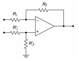
For a true differential amplifier, 𝑅′𝑖 is set to 𝑅𝑖 , and 𝑅′𝑓 is set to 𝑅𝑓 . A small potentiometer is typically placed in series with 𝑅′𝑓 in order to compensate for slight gain imbalances due to component tolerances. This makes it possible for the circuit’s common-mode rejection ratio to reach its maximum value. Another option for a simple difference amplifier is to set 𝑅′𝑖 plus 𝑅′𝑓 equal to 𝑅𝑖 . Doing so will maintain roughly equal input impedance between the two halves if two different input sources are used.
Once the divider is added, the output voltage is found by multiplying the differential input signal by 𝑅𝑓/𝑅𝑖 .
Example 4.2.15
Design a simple difference amplifier with an input impedance of 10 k Ω per leg, and a voltage gain of 26 dB.
First of all, converting 26 dB into ordinary form yields 20. Because 𝑅𝑖 sets 𝑍𝑖𝑛 , set 𝑅𝑖 = 10 k Ω , from the specifications.
![\[A_v = \frac{R_f}{R_i} \]](https://pressbooks.nscc.ca/app/uploads/quicklatex/quicklatex.com-142cfeee3b2492f9b370763f25a352f8_l3.png "Rendered by QuickLaTeX.com")
![\[R_f = \frac{A_v}{R_i} \]](https://pressbooks.nscc.ca/app/uploads/quicklatex/quicklatex.com-c84891f19d6c21017e8db682889a95a7_l3.png "Rendered by QuickLaTeX.com")
![\[R_f = 20\times 10 k \]](https://pressbooks.nscc.ca/app/uploads/quicklatex/quicklatex.com-105e10c69a58a6b80d83d798dc77d808_l3.png "Rendered by QuickLaTeX.com")
For equivalent inputs,
![\[R_i^{'} + R_f^{'} = R_i \]](https://pressbooks.nscc.ca/app/uploads/quicklatex/quicklatex.com-8aeb97ef6b8a5bab761fbcb59b68f3ff_l3.png "Rendered by QuickLaTeX.com")
![\[R_i^{'} + R_f^{'} = 10 k \]](https://pressbooks.nscc.ca/app/uploads/quicklatex/quicklatex.com-191e2546713ab5987c230361a49e78ae_l3.png "Rendered by QuickLaTeX.com")
Given that 𝐴𝑣 = 20,
![\[R_f^{'} = 20\times R_i^{'} \]](https://pressbooks.nscc.ca/app/uploads/quicklatex/quicklatex.com-e61254c9921290fee4dd04c8780f3047_l3.png "Rendered by QuickLaTeX.com")
Therefore,
![\[21\times R_i^{'} = 10 k \]](https://pressbooks.nscc.ca/app/uploads/quicklatex/quicklatex.com-56922315defe21553bc8e42cc8f0e651_l3.png "Rendered by QuickLaTeX.com")
![\[R_i^{'} = 476 \]](https://pressbooks.nscc.ca/app/uploads/quicklatex/quicklatex.com-0951e2c3dd596dcd0ceec5af895572b7_l3.png "Rendered by QuickLaTeX.com")
![\[R_f^{'} = 9.52 k \]](https://pressbooks.nscc.ca/app/uploads/quicklatex/quicklatex.com-06f4cf1237aa3903ef368fcfa451f294_l3.png "Rendered by QuickLaTeX.com")
The final result is shown in Figure 4.2.27 . As you will see later in Chapter Six, the differential amplifier figures prominently in another useful circuit, the instrumentation amplifier.

Adder/Subtractor
If inverting and noninverting summing amplifiers are combined using the differential amplifier topology, an adder/subtractor results. Normally, all resistors in an adder/subtractor are the same value. A typical adder/subtractor is shown in Figure 4.2.28 .
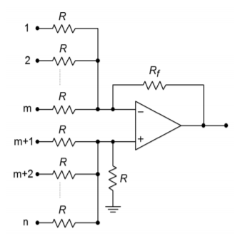
The inverting inputs number from 1 through 𝑚 , and the noninverting inputs number from 𝑚+1 through 𝑛 . The circuit can be analyzed by combining the preceding proofs of Equations 4.2.9 through 4.2.11 via the Superposition Theorem. The details are left as an exercise (Problem 4.45). When all resistors are equal, the input weightings are unity, and the output is found by:
![\[V_{out} = \sum_{i=m+1}^{n}{ V_{i n_i}} − \sum_{j=1}^{m}{V_{i n_j}} \]](https://pressbooks.nscc.ca/app/uploads/quicklatex/quicklatex.com-0efbc28cd399cd347d089d332b7a80af_l3.png "Rendered by QuickLaTeX.com")
(4.2.12)
In essence, you can think of the output voltage in terms of subtracting the inverting input summation from the noninverting input summation.
Adjustable Inverter/Noninverter
A unique adjustable gain amplifier is shown in Figure 4.2.29 . What makes this circuit interesting is that the gain is continuously variable between an inverting and noninverting maximum. For example, the gain might be set for a maximum of 10. A full turn of the potentiometer would swing the gain from +10 through -10. The exact middle setting would produce a gain of 0. In this way, a single knob controls both the phase and magnitude of the gain.
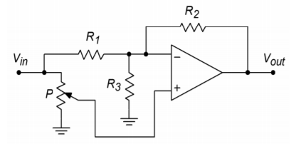
For the analysis of the circuit, refer to Figure 4.2.30 .
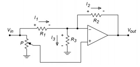
As you would expect, the gain of the circuit is defined as the ratio of the output to input voltages. It is important to note that unlike a normal inverting amplifier, the magnitude of the output voltage is not necessarily equal to the voltage across 𝑅2 . This is because the inverting terminal of the op amp is not normally a virtual ground. Instead, the voltage across 𝑅3 must also be considered. Because the two inputs of the op amp must be at approximately the same potential (i.e., 𝑉𝑒𝑟𝑟𝑜𝑟 must be 0), the voltage at the inverting terminal must be the same as the voltage tapped off of the potentiometer. Representing the potentiometer’s voltage divider factor as 𝑘 , we find:
![\[V_{out} = k V_{i n} -V_{R2} \]](https://pressbooks.nscc.ca/app/uploads/quicklatex/quicklatex.com-67b8fdc31bcd0a23cab09af5def6444a_l3.png "Rendered by QuickLaTeX.com")
(4.2.13)
The drop across 𝑅2 is simply 𝐼2𝑅2 . 𝐼2 is found by Kirchhoff’s Current Law and the appropriate voltage-resistor substitutions:
![\[I_2 = I_1 - I_3 \]](https://pressbooks.nscc.ca/app/uploads/quicklatex/quicklatex.com-656bccb56dc608819e075cb46c38fd35_l3.png "Rendered by QuickLaTeX.com")
![\[I_2 = \frac{V_{i n}−k V_{i n}}{R_1} - \frac{k V_{i n}}{R_3} \]](https://pressbooks.nscc.ca/app/uploads/quicklatex/quicklatex.com-f639229e6c2ef9480bea88e706712a3c_l3.png "Rendered by QuickLaTeX.com")
![\[I_2 = V_{i n}\left( \frac{1-k}{R_1} - \frac{k}{R_3}\right) \]](https://pressbooks.nscc.ca/app/uploads/quicklatex/quicklatex.com-0a50ab0b6cc1b0fba8cc574cbfab58cb_l3.png "Rendered by QuickLaTeX.com")
Thus, V_{R2} is found to be
![\[V_{R2} = V_{i n}\left( (1-k) \frac{R_2}{R_1} - k \frac{R_2}{R_3} \right) \]](https://pressbooks.nscc.ca/app/uploads/quicklatex/quicklatex.com-31459315f6d3e7631c706c8c4312734d_l3.png "Rendered by QuickLaTeX.com")
(4.2.14)
Combining Equations 4.2.13 and ??? and then solving for gain, we find
![\[A_v = k-\left( (1-k ) \frac{R_2}{R_1} -k \frac{R_2}{R_3} \right) \]](https://pressbooks.nscc.ca/app/uploads/quicklatex/quicklatex.com-28895507e58c4f479594064197705c56_l3.png "Rendered by QuickLaTeX.com")
![\[A_v = k-\left( \frac{R_2}{R_1} -k \frac{R_2}{R_1} -k \frac{R_2}{R_3} \right) \]](https://pressbooks.nscc.ca/app/uploads/quicklatex/quicklatex.com-a94f29772eb3226c7b2d24f616ef2fc5_l3.png "Rendered by QuickLaTeX.com")
![\[A_v =- \frac{R_2}{R_1} +k \left( 1+ \frac{R_2}{R_1} + k \frac{R_2}{R_3} \right) \]](https://pressbooks.nscc.ca/app/uploads/quicklatex/quicklatex.com-2791105afc108cc145faae10be8b0da6_l3.png "Rendered by QuickLaTeX.com")
The value of 𝑅3 is chosen so that 𝑅1=𝑅2||𝑅3 . This means that
![\[R_3 = \frac{1}{\frac{1}{R_1} - \frac{1}{R_2}} \]](https://pressbooks.nscc.ca/app/uploads/quicklatex/quicklatex.com-7d36a087c25db1f7e638eff0928b2b8c_l3.png "Rendered by QuickLaTeX.com")
Substituting this into our gain Equation and simplifying yields
![\[A_v = \frac{R_2}{R_1} (2k−1) \]](https://pressbooks.nscc.ca/app/uploads/quicklatex/quicklatex.com-69900bb8fb84514b199b80885a6f2879_l3.png "Rendered by QuickLaTeX.com")
In essence, the resistors 𝑅1 and 𝑅2 set the maximum gain. The potentiometer sets 𝑘 from 0 through 1. If 𝑘=1 , then 𝐴𝑣=𝑅2/𝑅1 , or maximum noninverting gain. When 𝑘=0 , then 𝐴𝑣=−𝑅2/𝑅1 , or maximum inverting gain. Finally, when the potentiometer is set to the mid-point, 𝑘=0.5 and 𝐴𝑣=0 .
- Most notably, operational transconductance amplifiers and digital to analog converters, which we will examine in Chapters Six and Twelve, respectively. ↵
