
1.4 JFET Biasing
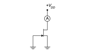
There are several different ways of biasing a JFET. For many configurations, 𝐼𝐷𝑆𝑆 and 𝑉𝐺𝑆(𝑜𝑓𝑓) will be needed. A simple way to measure these parameters in the lab is shown in Figure 1.4.1. To measure 𝐼𝐷𝑆𝑆 we simply ground the gate and source terminals as this forces 𝑉𝐺𝑆 to be 0 V. We insert an ammeter between 𝑉𝐷𝐷 and the drain, and then set 𝑉𝐷𝐷 to a value higher than 𝑉𝑃 (+15 VDC generally being sufficient). The resulting ammeter reading is 𝐼𝐷𝑆𝑆. Obtaining 𝑉𝐺𝑆(𝑜𝑓𝑓) is only slightly more work. Leaving the ammeter in the drain, unhook the gate from ground and instead connect it to an adjustable negative power supply. Turn the supply more negative until the ammeter reads zero (practically speaking, < 1% of 𝐼𝐷𝑆𝑆). At that point the voltage source will be equal to 𝑉𝐺𝑆(𝑜𝑓𝑓).
DC Model
Before we begin examining the bias circuits themselves, we need a basic DC model of the JFET. A model sufficient for our analyses is shown in Figure 1.4.2.
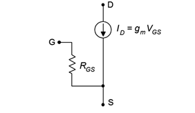
The model consists of a voltage-controlled current source, 𝐼𝐷, that is equal to the product of the gate-source voltage, 𝑉𝐺𝑆, and the transconductance, 𝑔𝑚. The resistance between the gate and source, 𝑅𝐺𝑆, is that of the reverse-biased PN junction, in other words, ideally infinity for DC. As a consequence, in most practical circuits we can assume that gate current, 𝐼𝐺, is zero. Therefore, 𝐼𝐷=𝐼𝑆.
Constant Voltage Bias
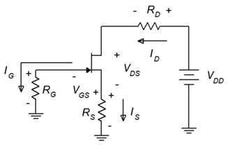
The simplest form of bias is the constant voltage bias. The prototype is shown in Figure 1.4.3 with current directions and voltage polarities shown.
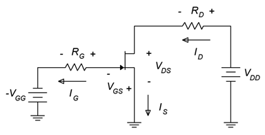
This is a fairly straightforward design using only a couple of resistors and power sources. Figure 1.4.4 shows the same circuit but with the JFET model inserted, ready for analysis.

Ultimately, the goal here is to determine a means for finding the transistor’s drain current and drain-source voltage, along with the potentials across any other components.
To begin, consider the gate-source loop. By KVL, the 𝑉𝐺𝐺 source must drop across 𝑅𝐺 and the gate-source junction, 𝑉𝐺𝑆.
![\[V_{G G} = V_{R_G} +V_{GS} \]](https://pressbooks.nscc.ca/app/uploads/quicklatex/quicklatex.com-50228ba4c95ad53c53c4413418e791d9_l3.png "Rendered by QuickLaTeX.com")
![\[V_{G G} = I_G R_G+V_{GS} \]](https://pressbooks.nscc.ca/app/uploads/quicklatex/quicklatex.com-d3b77fcece5f24fecabc931c418568bf_l3.png "Rendered by QuickLaTeX.com")
𝐼𝐺 is approximately zero so this simplifies to
![\[V_{GS} = V_{G G} \]](https://pressbooks.nscc.ca/app/uploads/quicklatex/quicklatex.com-e70f84a08ce71af1f00be501ac709667_l3.png "Rendered by QuickLaTeX.com")
Given the transconductance, 𝑔𝑚gm, we can find 𝐼𝐷. Alternately, 𝐼𝐷 may be found using Equation 1.2.1 along with the device parameters 𝐼𝐷𝑆𝑆 and 𝑉𝐺𝑆(𝑜𝑓𝑓). For this circuit, the latter technique tends to be more practical. Once 𝐼𝐷 is found, the voltage drop across 𝑅𝐷 may be found, and then 𝑉𝐷𝑆 is determined from KVL.
Example 1.4.1
For the circuit of Figure 1.4.5, determine 𝐼𝐷 and 𝑉𝐷𝑆. Assume 𝐼𝐷𝑆𝑆 = 10 mA and 𝑉𝐺𝑆(𝑜𝑓𝑓) = −5 V.
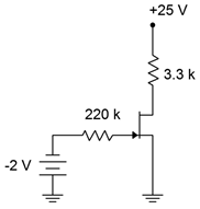
First, because 𝐼𝐺≈0, the drop across 𝑅𝐺 is ≈0 and 𝑉𝐺𝑆=𝑉𝐺𝐺. Using Equation 1.2.1
![\[I_D = I_{DSS} \left( 1 - \frac{V_{GS}}{V_{GS (off )}} \right)^2 \]](https://pressbooks.nscc.ca/app/uploads/quicklatex/quicklatex.com-e385c0981c41e62126e8dfe37359350c_l3.png "Rendered by QuickLaTeX.com")
![\[I_D = 10 mA \left( 1 - \frac{-2 V}{-5V} \right)^2 \]](https://pressbooks.nscc.ca/app/uploads/quicklatex/quicklatex.com-1f14baa96990c9a2fa6d5fcd1f6ff853_l3.png "Rendered by QuickLaTeX.com")
![\[I_D = 3.6 mA \]](https://pressbooks.nscc.ca/app/uploads/quicklatex/quicklatex.com-6558739686fff7406b1350e7c1e0717f_l3.png "Rendered by QuickLaTeX.com")
Looking at the drain-source loop, KVL shows
![\[V_{DD} = I_D R_D +V_{DS} \]](https://pressbooks.nscc.ca/app/uploads/quicklatex/quicklatex.com-3cb275aa64a7001fab5e17001d27f69a_l3.png "Rendered by QuickLaTeX.com")
![\[V_{DS} = V_{DD} -I_D R_D \]](https://pressbooks.nscc.ca/app/uploads/quicklatex/quicklatex.com-50051dae31faf245036d73c2478a034f_l3.png "Rendered by QuickLaTeX.com")
![\[V_{DS} = 25V -3.6mA \times 3.3k \Omega \]](https://pressbooks.nscc.ca/app/uploads/quicklatex/quicklatex.com-36f5b60bb8271140011b1014a1bcc576_l3.png "Rendered by QuickLaTeX.com")
![\[V_{DS} = 13.1 V \]](https://pressbooks.nscc.ca/app/uploads/quicklatex/quicklatex.com-0f1150581a2da3dc195158d9cc72604a_l3.png "Rendered by QuickLaTeX.com")
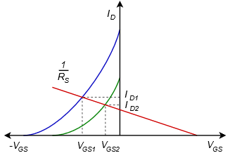
While the computation for the constant voltage bias is relatively simple, it does not exhibit a stable Q point. For example, if Example 1.4.1 is repeated with another JFET, this one with 𝐼𝐷𝑆𝑆 = 12 mA and 𝑉𝐺𝑆(𝑜𝑓𝑓) = −6 V, the results are starkly different: 𝐼𝐷 grows to 5.33 mA and 𝑉𝐷𝑆 shrinks to 7.4 V. These are considerable changes given the relatively modest shifts in the device parameters. In this regard, the constant voltage bias is reminiscent of the simple base bias configuration used with BJTs.
To get a better understanding of the Q point stability issue, refer to Figure 1.4.6.
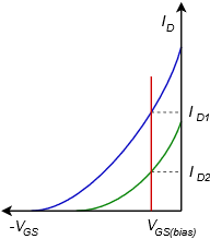
Characteristic curves are plotted here for two different devices, one in green and one in blue. These represent the sort of device parameter variations we might expect to see across a product model. The fixed value of gate bias voltage is shown in red. From this graph it should be obvious that this form of bias will produce a wide variation in drain current, and thus, is not a good choice for applications that require a stable Q point. If the application does not have this requirement, constant voltage bias offers the advantage of requiring a minimum of components.
Self Bias
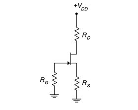
Self bias uses a small number of components and only a single power supply, yet it offers better stability than constant voltage bias. The name comes from the fact that the drain current will be used to create a voltage drop that sets up the gate-source, hence the circuit “biases itself”. It is also referred to as automatic bias. The self bias prototype is shown in Figure 1.4.7.
Once again, we may assume that 𝐼𝐺 is 0. As 𝑅𝐺 is connected directly to ground, this means that 𝑉𝐺≈0. This being true, inspection of the schematic reveals that the magnitude of 𝑉𝐺𝑆 must be the same as the voltage across 𝑅𝑆. Because 𝐼𝐷=𝐼𝑆 then
![\[V_{GS} = -I_D R_S \]](https://pressbooks.nscc.ca/app/uploads/quicklatex/quicklatex.com-9813d30bc0d15f2fe7827ba68fef48c2_l3.png "Rendered by QuickLaTeX.com")
(1.4.1)
This value of 𝑉𝐺𝑆 is what generates the drain current. The definition is self-referential. This being the case, how do we analyze the circuit? A proper derivation of the equation for drain current is not trivial. We start with the characteristic equation (Equation 11.2.1) and expand it.
![\[I_D = I_{DSS}\left ( 1 - \frac{V_{GS}}{V_{GS (off )}} \right)^2 \]](https://pressbooks.nscc.ca/app/uploads/quicklatex/quicklatex.com-f1c988d4f09a2475d809e7ab262d47c2_l3.png "Rendered by QuickLaTeX.com")
![\[I_D = I_{DSS} \left( 1 - \frac{2V_{GS}}{V_{GS (off )}} + \frac{{V_{GS}}^2}{{V_{GS(off )}}^2} \right) \]](https://pressbooks.nscc.ca/app/uploads/quicklatex/quicklatex.com-e3104ac418e7636d80643a5c731205e3_l3.png "Rendered by QuickLaTeX.com")
![\[I_D = I_{DSS} - \frac{2 I_{DSS} V_{GS}}{V_{GS (off )}} + \frac{I_{DSS} {V_{GS}}^2}{{V_{GS (off )}}^2} \]](https://pressbooks.nscc.ca/app/uploads/quicklatex/quicklatex.com-e46e7b8ed74a1250ea1503c82cd57426_l3.png "Rendered by QuickLaTeX.com")
Substitute using Equation 1.2.2
![\[g_{m0} =- \frac{2 I_{DSS}}{V_{GS(off )}} \]](https://pressbooks.nscc.ca/app/uploads/quicklatex/quicklatex.com-e93d435cc5258e1422e1e601424cc52a_l3.png "Rendered by QuickLaTeX.com")
![\[I_D = I_{DSS} +g_{m0} V_{GS} + \frac{I_{DSS} {V_{GS}}^2}{{V_{GS (off )}}^2} \]](https://pressbooks.nscc.ca/app/uploads/quicklatex/quicklatex.com-f75d36aca6bb689cc3005b501913f4b8_l3.png "Rendered by QuickLaTeX.com")
Using Equation 1.4.1 this can be expanded to
![\[I_D = I_{DSS} -g_{m0} I_D R_S + \frac{I_{DSS} {I_D}^2 {R_S}^2}{{V_{GS (off )}}^2} \]](https://pressbooks.nscc.ca/app/uploads/quicklatex/quicklatex.com-6826cd93649613d91a34903b240a4704_l3.png "Rendered by QuickLaTeX.com")
Rearranging yields
![\[0 = \frac{I_{DSS} {R_S}^2}{{V_{GS (off )}}^2} {I_D}^2 - (1 +g_{m0} R_S )I_D +I_{DSS} \]](https://pressbooks.nscc.ca/app/uploads/quicklatex/quicklatex.com-ac5b55960800ef435345086b97738681_l3.png "Rendered by QuickLaTeX.com")
This is a quadratic equation in the form 𝑎𝑥2+𝑏𝑥+𝑐ax2+bx+c and can be solved using the quadratic formula:
![\[y = \frac{−b\pm \sqrt{b^2−4ac}}{2a} \]](https://pressbooks.nscc.ca/app/uploads/quicklatex/quicklatex.com-118453ba26321c3132ea9f5df0ee33b6_l3.png "Rendered by QuickLaTeX.com")
The positive option in the numerator may be ignored as this occurs or 𝑉𝐺𝑆 beyond 𝑉𝐺𝑆(𝑜𝑓𝑓). The result is
![\[I_D = 2 I_{DSS} \left( \frac{1+g_{m0} R_S -\sqrt{1+2 g_{m0} R_S}}{( g_{m0} R_S )^2} \right) \]](https://pressbooks.nscc.ca/app/uploads/quicklatex/quicklatex.com-45267b14c2dd161beb8fe20146ab45fd_l3.png "Rendered by QuickLaTeX.com")
(1.4.2)
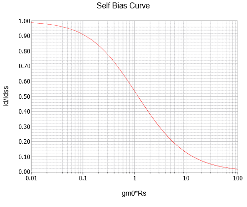
Although this is an accurate analytical solution, it’s certainly not the sort of equation most people want to memorize or derive as needed. As the 𝑔𝑚0𝑅𝑆 term is repeated in this equation multiple times, it is useful to plot this equation in terms of normalized 𝐼𝐷 versus 𝑔𝑚0𝑅𝑆. This curve is plotted in Figure 1.4.8.
The value of 𝑔𝑚0𝑅𝑆 is found on the horizontal axis, traced up to the curve and then over to the normalized 𝐼𝐷 ratio. This number is multiplied by 𝐼𝐷𝑆𝑆 to determine the value of 𝐼𝐷.
Example 1.4.2
Determine 𝐼𝐷 and 𝑉𝐷𝑆 for the circuit shown in Figure 11.4.9. Assume 𝐼𝐷𝑆𝑆 = 10 mA and 𝑉𝐺𝑆(𝑜𝑓𝑓) = −4 V.

Using the graphical method, first determine 𝑔𝑚0𝑅𝑆.
![\[g_{m0} =- \frac{2 I_{DSS}}{V_{GS (off )}} \]](https://pressbooks.nscc.ca/app/uploads/quicklatex/quicklatex.com-b77a0a7208e012f3272aba5fd5232900_l3.png "Rendered by QuickLaTeX.com")
![\[g_{m0} =- \frac{2 \times 10 mA}{−4 V} \]](https://pressbooks.nscc.ca/app/uploads/quicklatex/quicklatex.com-b1d3fd146ea4f5bddf76c1fc5f5be6ba_l3.png "Rendered by QuickLaTeX.com")
![\[g_{m0} = 5mS \]](https://pressbooks.nscc.ca/app/uploads/quicklatex/quicklatex.com-29b5298bb44582f428dfaf9d0a1fd6e7_l3.png "Rendered by QuickLaTeX.com")
Therefore 𝑔𝑚0𝑅𝑆 = 5 mS ⋅ 2.2 k Ω=11. The self bias graph yields approximately 0.12 for the normalized current ratio. Therefore
![\[I_D = 0.12 I_{DSS} \]](https://pressbooks.nscc.ca/app/uploads/quicklatex/quicklatex.com-7e3f3e069988418f2903834f8531d514_l3.png "Rendered by QuickLaTeX.com")
![\[I_D = 0.12 \times 10 mA \]](https://pressbooks.nscc.ca/app/uploads/quicklatex/quicklatex.com-f63e583cf535e9744b371b46a423adba_l3.png "Rendered by QuickLaTeX.com")
![\[I_D = 1.2mA \]](https://pressbooks.nscc.ca/app/uploads/quicklatex/quicklatex.com-07b852a4d9fd591ff201d50259775d39_l3.png "Rendered by QuickLaTeX.com")
Using Ohm’s law and KVL
![\[V_D = V_{DD} -I_D R_D \]](https://pressbooks.nscc.ca/app/uploads/quicklatex/quicklatex.com-5ade6b8d53f7379c28a13d6b9031ff4c_l3.png "Rendered by QuickLaTeX.com")
![\[V_D = 20 V-1.2mA \times 3.9 k\Omega \]](https://pressbooks.nscc.ca/app/uploads/quicklatex/quicklatex.com-f9f7e48b177f60c004b72738e881e234_l3.png "Rendered by QuickLaTeX.com")
![\[V_D = 15.32V \]](https://pressbooks.nscc.ca/app/uploads/quicklatex/quicklatex.com-b21024a26f06cf30991d3149a4b1feca_l3.png "Rendered by QuickLaTeX.com")
![\[V_S = I_D R_S \]](https://pressbooks.nscc.ca/app/uploads/quicklatex/quicklatex.com-7385e6cba03faeb6727b0d26cbf7ed06_l3.png "Rendered by QuickLaTeX.com")
![\[V_S = 1.2mA \times 2.2 k\Omega \]](https://pressbooks.nscc.ca/app/uploads/quicklatex/quicklatex.com-c00ea24c273dae333df0e7939bb83bfc_l3.png "Rendered by QuickLaTeX.com")
![\[V_S = 2.64 V \]](https://pressbooks.nscc.ca/app/uploads/quicklatex/quicklatex.com-5dcd09a480b39ded1c6d18df8c39ed52_l3.png "Rendered by QuickLaTeX.com")
![\[V_{DS} = V_D -V_S \]](https://pressbooks.nscc.ca/app/uploads/quicklatex/quicklatex.com-0d63582ed68708b72c8395a65789348a_l3.png "Rendered by QuickLaTeX.com")
![\[V_{DS} = 15.32 V -2.64 V \]](https://pressbooks.nscc.ca/app/uploads/quicklatex/quicklatex.com-78a6f7e79663c4aff81cf3422ef58885_l3.png "Rendered by QuickLaTeX.com")
![\[V_{DS} = 12.68 V \]](https://pressbooks.nscc.ca/app/uploads/quicklatex/quicklatex.com-04401896cf0304af0e1eb811d90d76a9_l3.png "Rendered by QuickLaTeX.com")
An alternate technique is to make an initial guess for 𝑉𝐺𝑆, typically one half of 𝑉𝐺𝑆(𝑜𝑓𝑓). The value of 𝐼𝐷 is then computed from the characteristic equation (Equation 1.2.1) and compared with the Ohm’s law relation, Equation 1.4.1, rewritten as 𝐼𝐷=−𝑉𝐺𝑆/𝑅𝑆. Chances are, the two results will not agree so adjust the 𝑉𝐺𝑆 estimate and repeat the process. If done properly, the currents should be closer. Iterate this process until you converge on the answer.
To use this technique for the preceding problem we’d start by assuming 𝑉𝐺𝑆 = −2 V (half of 𝑉𝐺𝑆(𝑜𝑓𝑓))). Using this in Equation 1.2.1 yields 𝐼𝐷 = 2.5 mA, while using Equation 1.4.1 produces 𝐼𝐷 = 910 𝜇A. Obviously the initial estimate was not correct. The second estimate for 𝑉𝐺𝑆VGS needs to increase negatively as this will decrease the result from Equation 1.2.1 and increase the result from Equation 1.4.1, hopefully meeting in the middle. We might try −2.5 volts. This will yield 1.4 mA from Equation 1.2.1 and 1.14 mA from Equation 1.4.1. As the gap has narrowed, the adjustment for the third estimate will be smaller, so we could try −2.6 volts. This would be relatively close to the value as computed in Example 1.4.2 (𝑉𝐺𝑆=−𝑉𝑆).
This approximation technique also offers a clue as to how self bias gains stability over constant voltage bias. If for some reason 𝐼𝐷 was to increase, this would create a larger voltage drop across 𝑅𝑆. Because this voltage is the same magnitude as 𝑉𝐺𝑆, this means that 𝑉𝐺𝑆 grows negatively. A more negative 𝑉𝐺𝑆 reduces 𝐼𝐷, thus opposing the initial change in drain current. This feedback mechanism is similar in function to the BJT collector feedback bias. The stability issue is visualized in Figure 1.4.1.

Two device curves are plotted to represent parameter variation (green and blue). Equation 1.4.1 shows the relationship between 𝐼𝐷 and 𝑉𝐺𝑆. If we put this in the form 𝑦=𝑚𝑥+𝑏y=mx+b, we find that the line goes through the origin and has a slope of 1/𝑅𝑆. This line is plotted in red. Where the line intersects the device curve yields the drain current and gate-source voltage for that particular device. Unlike constant voltage bias, self bias shifts some variation over to 𝑉𝐺𝑆, making 𝐼𝐷 more stable. In fact, if there is a particular design target for 𝐼𝐷 or 𝑉𝐺𝑆, a rearrangement of Equation 1.4.1 can be used to find the needed value of 𝑅𝑆 along with the characteristic curve or equation.
![\[R_S =- \frac{V_{GS}}{I_D} \]](https://pressbooks.nscc.ca/app/uploads/quicklatex/quicklatex.com-0c9b379c7ae4224d53f4774f67520a25_l3.png "Rendered by QuickLaTeX.com")
For example, if a certain 𝐼𝐷 is desired, this value could be used with Equation 1.2.1 to determine the corresponding 𝑉𝐺𝑆. These values are then used to find the required 𝑅𝑆. Alternately, the normalized values could be obtained via Figure 11.2.4.
Example 1.4.3
Determine a value for 𝑅𝑆 to set 𝑉𝐺𝑆 = −2 V for the circuit shown in Figure 1.4.11. Assume 𝐼𝐷𝑆𝑆= 20 mA and 𝑉𝐺𝑆(𝑜𝑓𝑓) = −4 V.
We can determine the drain current using Equation 1.2.1.
![\[I_D = I_DSS \left( 1 - \frac{V_{GS}}{V_{GS (off )}} \right)^2 \]](https://pressbooks.nscc.ca/app/uploads/quicklatex/quicklatex.com-edef9c8238893bedad01bd81681ea9a7_l3.png "Rendered by QuickLaTeX.com")
![\[I_D = 20 mA \left( 1 - \frac{-2V}{-4V} \right)^2 \]](https://pressbooks.nscc.ca/app/uploads/quicklatex/quicklatex.com-bfb42ac869b91f0df865ae4c515882c0_l3.png "Rendered by QuickLaTeX.com")
![\[I_D = 5 mA \]](https://pressbooks.nscc.ca/app/uploads/quicklatex/quicklatex.com-05f39fde280df42514011212f8f6abab_l3.png "Rendered by QuickLaTeX.com")
![\[R_S =− \frac{-2 V}{5mA} \]](https://pressbooks.nscc.ca/app/uploads/quicklatex/quicklatex.com-3b431d0b21ceae9233604b630fabafdf_l3.png "Rendered by QuickLaTeX.com")
![\[R_S = 400 \Omega \]](https://pressbooks.nscc.ca/app/uploads/quicklatex/quicklatex.com-8fdd5965eaa27f8cd5bf1d1bcfbc2281_l3.png "Rendered by QuickLaTeX.com")
In sum, self bias is a minimal parts count circuit that offers modest stability. The stability can be improved with the addition of other components, as we shall see with the next bias configuration.
Combination Bias
The combination bias configuration (AKA source bias) is based on self bias but adds a negative power supply connected to 𝑅𝑆, hence its name. This will enhance the stability of 𝐼𝐷, 𝑉𝐷𝑆 and 𝑔𝑚. The combination bias prototype is shown in Figure 1.4.12.

The analysis is similar to that of self bias but with one major twist: the source power supply increases the voltage drop across 𝑅𝑆. This stabilizes the voltage (and hence, the current) because it is no longer equal to −𝑉𝐺𝑆, but rather
![\[V_{R_S} = I_D R_S =|V_{GS}|+|V_{SS}| \]](https://pressbooks.nscc.ca/app/uploads/quicklatex/quicklatex.com-7eb2caea0c6d2b6523fe1ffe2d034bee_l3.png "Rendered by QuickLaTeX.com")
(1.4.3)
If 𝑉𝑆𝑆≫𝑉𝐺𝑆, then we can approximate 𝐼𝐷 as 𝑉𝑆𝑆/𝑅𝑆. As with self bias, an analytical solution for 𝐼𝐷 is possible. In order to do so, we would begin with the characteristic equation and Equation 1.4.3. The derivation is left as an exercise.
![\[I_D = 2 I_{DSS} \left( \frac{1+g_{m0} R_S (1+k )-\sqrt{1+2 g_{m0}R_S (1+k)}}{( g_{m0} R_S )^2} \right) \]](https://pressbooks.nscc.ca/app/uploads/quicklatex/quicklatex.com-e7a0b4f95575f3ac997df30ee6ad192e_l3.png "Rendered by QuickLaTeX.com")
(1.4.4)
The formula is very similar to the self bias formula but with the addition of a factor, 𝑘. 𝑘 is a “swamping factor” and is defined as the ratio of 𝑉𝑆𝑆 to 𝑉𝐺𝑆(𝑜𝑓𝑓). If 𝑘=0, there is no source power supply and the formula reverts back to the simpler self bias formula. On the other hand, if 𝑘 is very large, 𝐼𝐷≈𝑉𝑆𝑆/𝑅𝑆.
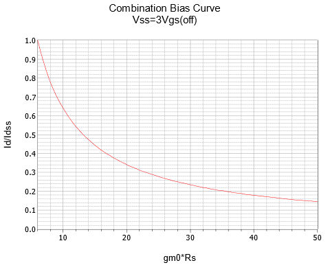
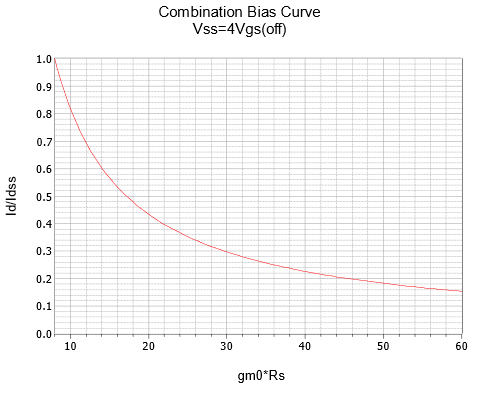
As was the case with self bias, we can plot Equation 1.4.4 using the 𝑔𝑚0𝑅𝑆 factor. A series of three plots for 𝑘 = 2, 3 and 4 are rendered in Figure 1.4.13.[1]

Example 1.4.4
Determine 𝐼𝐷 and 𝑉𝐷𝑆 for the circuit shown in Figure 1.4.14. Assume 𝐼𝐷𝑆𝑆 = 12 mA and 𝑉𝐺𝑆(𝑜𝑓𝑓) = −4 V.

Using the graphical method, first determine 𝑔𝑚0𝑅𝑆.
![\[g_{m0} = - \frac{2 \times 12 mA}{-4V} \]](https://pressbooks.nscc.ca/app/uploads/quicklatex/quicklatex.com-83024b62f2aa6fe3a75345d905e196bf_l3.png "Rendered by QuickLaTeX.com")
![\[g_{m0} = 6mS \]](https://pressbooks.nscc.ca/app/uploads/quicklatex/quicklatex.com-3ab34c901c1963881eb3e2b85181fe48_l3.png "Rendered by QuickLaTeX.com")
Therefore 𝑔𝑚0𝑅𝑆 = 6 mS ⋅ 3.3 k Ω = 19.8. The swamping ratio, 𝑘, is 𝑉𝑆𝑆/𝑉𝐺𝑆(𝑜𝑓𝑓)=−8/−4=2. This requires the graph in Figure 1.4.13𝑎. This graph yields approximately 0.25 for the normalized current ratio. Therefore
![\[I_D = 0.25 I_{DSS} \]](https://pressbooks.nscc.ca/app/uploads/quicklatex/quicklatex.com-f7011612cd37c01da7ca4e9f67c369ee_l3.png "Rendered by QuickLaTeX.com")
![\[I_D = 0.25 \times 12 mA \]](https://pressbooks.nscc.ca/app/uploads/quicklatex/quicklatex.com-801abac965d4b2783badbe57bea98750_l3.png "Rendered by QuickLaTeX.com")
![\[I_D = 3mA \]](https://pressbooks.nscc.ca/app/uploads/quicklatex/quicklatex.com-fbff2c86a44bd73f6e33306f2d7160cc_l3.png "Rendered by QuickLaTeX.com")
Using Ohm’s law and KVL
![\[V_D = V_{DD} - I_D R_D \]](https://pressbooks.nscc.ca/app/uploads/quicklatex/quicklatex.com-c357c833e0a09b1c2f8407ddcdf3bf99_l3.png "Rendered by QuickLaTeX.com")
![\[V_D = 24 V-3mA \times 4.7k\Omega \]](https://pressbooks.nscc.ca/app/uploads/quicklatex/quicklatex.com-b5d9263c286dd4909a6cb0bb14c2145a_l3.png "Rendered by QuickLaTeX.com")
![\[V_D = 9.9 V \]](https://pressbooks.nscc.ca/app/uploads/quicklatex/quicklatex.com-f526ff1f8acccba9eacd842d81266a60_l3.png "Rendered by QuickLaTeX.com")
![\[V_S = V_{SS}+I_D R_S \]](https://pressbooks.nscc.ca/app/uploads/quicklatex/quicklatex.com-217c4a7fdcb803d7ce35cc5b3d9bd55e_l3.png "Rendered by QuickLaTeX.com")
![\[V_S =-8V+3mA \times 3.3 k\Omega \]](https://pressbooks.nscc.ca/app/uploads/quicklatex/quicklatex.com-81b2318c257216f716907c2685772f98_l3.png "Rendered by QuickLaTeX.com")
![\[V_S = 1.9V \]](https://pressbooks.nscc.ca/app/uploads/quicklatex/quicklatex.com-87b04281a8030edc39584f88c875a85d_l3.png "Rendered by QuickLaTeX.com")
![\[V_{DS} = 9.9 V -1.9V \]](https://pressbooks.nscc.ca/app/uploads/quicklatex/quicklatex.com-c2d5556d4b00665f08738ce33b779761_l3.png "Rendered by QuickLaTeX.com")
![\[V_{DS} = 8 V \]](https://pressbooks.nscc.ca/app/uploads/quicklatex/quicklatex.com-8a166020dac46368e734fdae6b6e36e5_l3.png "Rendered by QuickLaTeX.com")
As a crosscheck, using Equation 1.4.4 yields 3.028 mA for 𝐼𝐷. The deviation is no doubt due to inaccuracy in reading the graph. In any case, using this value of drain current we find 𝑉𝑆 to be 1.992 volts, a little higher than calculated above. This indicates that 𝑉𝐺𝑆 is −1.992 volts (because 𝑉𝐺≈0). If we plug this value of 𝑉𝐺𝑆 into Equation 1.2.1, 𝐼𝐷=3.024 mA; an excellent match with the deviation being due to accumulated rounding errors.
In order to show the increased Q point stability of the combination bias, we’ll repeat the preceding problem using a JFET with a significantly lower 𝐼𝐷𝑆𝑆.
Example 1.4.5
Determine 𝐼𝐷 for the circuit shown in Figure 1.4.14. Assume 𝐼𝐷𝑆𝑆 = 8 mA and 𝑉𝐺𝑆(𝑜𝑓𝑓) = −4 V.
For this version we’ll use Equation 1.4.4. First determine 𝑔𝑚0𝑅𝑆.
![\[g_{m0} =- \frac{2 \times 8mA}{-4 V} \]](https://pressbooks.nscc.ca/app/uploads/quicklatex/quicklatex.com-99f57c3f00b420f4fce296a509ac3b4c_l3.png "Rendered by QuickLaTeX.com")
![\[g_{m0} = 4 mS \]](https://pressbooks.nscc.ca/app/uploads/quicklatex/quicklatex.com-e3a776e7667a037333dd92518579a3a2_l3.png "Rendered by QuickLaTeX.com")
Therefore 𝑔𝑚0𝑅𝑆 = 4 mS ⋅ 3.3 k Ω=13.2. The swamping ratio, 𝑘, is 𝑉𝑆𝑆/𝑉𝐺𝑆(𝑜𝑓𝑓)=−8/−4=2.
![\[I_D =2 I_{DSS} \left( \frac{1+g_{m0} R_S (1+k) -\sqrt{1+2 g_{m0} R_S (1+k )}}{( g_{m0} R_S )^2} \right) \]](https://pressbooks.nscc.ca/app/uploads/quicklatex/quicklatex.com-878325920ed9f784332c889dfc23c676_l3.png "Rendered by QuickLaTeX.com")
![\[I_D = 2 \times 8mA \left( \frac{1+13.2(1+2)-\sqrt{1+2 \times 13.2(1+2)}}{(13.2)^2} \right) \]](https://pressbooks.nscc.ca/app/uploads/quicklatex/quicklatex.com-f2fe595c9d5d6d12eeb2bc9a13587793_l3.png "Rendered by QuickLaTeX.com")
![\[I_D =2.906 mA \]](https://pressbooks.nscc.ca/app/uploads/quicklatex/quicklatex.com-96cc7ad7f781ad173f8c72f9ab9efb5e_l3.png "Rendered by QuickLaTeX.com")
For the graphical method, a reasonable estimate for the normalized 𝐼𝐷 would be around 0.36, yielding a drain current of 2.88 mA. Stability is apparent because the drain current has dropped only a few percent in spite of the fact that 𝐼𝐷𝑆𝑆 decreased by 33%.
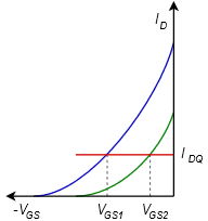
The graph of Figure 1.4.15 illustrates nicely the increased stability of the Q point. Once again, we plot two representative device curves in green and blue. As was the case with self bias, a plot line can be drawn, the slope of which is equal to the reciprocal of 𝑅𝑆. This plot line does not go though the origin, though. Instead, the 𝑥x axis intercept is the voltage |𝑉𝑆𝑆|. Thus, the red plot line is shifted along the 𝑉𝐺𝑆 axis.
As can be seen in the graph, the variation in 𝐼𝐷 is reduced (although at the expense of variation in 𝑉𝐺𝑆). For large values of 𝑉𝑆𝑆 with correspondingly large values of 𝑅𝑆, the bias plot line becomes nearly horizontal, indicating a very stable Q point. With two variables in play, this bias proves to be very flexible. It can also be realized by using a positive voltage divider at the gate and removing 𝑉𝑆𝑆 (returning 𝑅𝑆 to ground).
Constant Current Bias
The most stable bias for JFETs relies, oddly enough, on a current source made with a BJT. It is called constant current bias, yet another imaginative tag. Interestingly, although this will keep the Q point very stable, a fixed 𝐼𝐷 does not guarantee the most stable value of voltage gain. In fact, it might be easier to achieve that goal using combination bias. The prototype constant current bias circuit is shown in Figure 1.4.16. An NPN BJT is used for an N-channel JFET and a PNP would be used with a P-channel JFET, typically driven from above (i.e., circuit flipped top to bottom).

Ignoring the JFET for a moment, the BJT is configured as in two-supply emitter bias. In this case the base is tied directly to ground, leaving the emitter at about −0.7 VDC. The remainder of the 𝑉𝐸𝐸 supply drops across 𝑅𝐸, establishing the emitter current. As the collector is connected directly to the JFET’s source terminal, this means that 𝐼𝑆≈𝐼𝐸. The source current winds up being just as stable as the emitter current, which we have already seen is very stable. The only requirement is that 𝐼𝐸 should not be programmed to be larger than 𝐼𝐷𝑆𝑆. This being true, 𝐼𝐷 will set up a corresponding 𝑉𝐺𝑆. This also establishes 𝑉𝑆 because 𝑉𝐺≈0. Therefore, the source terminal will be a small positive voltage and this is precisely what the BJT needs in order to guarantee that its collector-base junction is reverse-biased.
Computation of circuit currents and voltages is straightforward and does not involve the use of graphical aides. The first step is to examine the BJT’s emitter loop and determine 𝐼𝐸. Once this is found, 𝐼𝑆 and 𝐼𝐷 are known, and all remaining component potentials may be found using Ohm’s law and KVL.
This technique does not involve the calculation of 𝑉𝐺𝑆. In fact, because 𝐼𝐷 is very stable, 𝑉𝐺𝑆 will show the widest variation of all biasing circuits when the JFET is changed. If 𝑉𝐺𝑆 is needed, it can be determined via a little algebraic manipulation on Equation 1.2.1.
Example 1.4.6
Determine 𝐼𝐷, 𝑉𝐷𝑆 and 𝑉𝐺𝑆 in the circuit of Figure 1.4.17. 𝐼𝐷𝑆𝑆 = 15 mA and 𝑉𝐺𝑆(𝑜𝑓𝑓) = −3 V.

We begin by finding 𝐼𝐸.
![\[I_E = \frac{|V_{EE}|-0.7V}{R_E} \]](https://pressbooks.nscc.ca/app/uploads/quicklatex/quicklatex.com-0fe4f75540156256eb9d8aee1cdd28c9_l3.png "Rendered by QuickLaTeX.com")
![\[I_E = \frac{10V -0.7V}{3.6k \Omega} \]](https://pressbooks.nscc.ca/app/uploads/quicklatex/quicklatex.com-4e27b15808b29ec71036289badc0deb9_l3.png "Rendered by QuickLaTeX.com")
![\[I_E = 2.58mA \]](https://pressbooks.nscc.ca/app/uploads/quicklatex/quicklatex.com-703046d5ba4e9b00c8dd127dc58d37ce_l3.png "Rendered by QuickLaTeX.com")
𝐼𝐸 is the same as 𝐼𝑆 and 𝐼𝐷, therefore
![\[V_D = 20 V -2.58 mA \times 4.7 k\Omega \]](https://pressbooks.nscc.ca/app/uploads/quicklatex/quicklatex.com-747062430ff47d5570ce0a99c278618b_l3.png "Rendered by QuickLaTeX.com")
![\[V_D = 7.87V \]](https://pressbooks.nscc.ca/app/uploads/quicklatex/quicklatex.com-d95f2d9b1aa74af14cc260f9cc077e8c_l3.png "Rendered by QuickLaTeX.com")
To find 𝑉𝑆 we note that 𝑉𝑆=−𝑉𝐺𝑆 and rearrange Equation 1.2.1.
![\[V_{GS} = V_{GS (off )} \left( 1 - \sqrt{\frac{I_D}{I_{DSS}}} \right) \]](https://pressbooks.nscc.ca/app/uploads/quicklatex/quicklatex.com-c3700993d69cc0102f25f66d3062b4b6_l3.png "Rendered by QuickLaTeX.com")
![\[V_{GS} = -3 V \left(1 - \sqrt{\frac{2.58 mA}{15 mA}} \right) \]](https://pressbooks.nscc.ca/app/uploads/quicklatex/quicklatex.com-d27caa07bbece15760e4581e59950128_l3.png "Rendered by QuickLaTeX.com")
![\[V_{GS} =-1.24 V \]](https://pressbooks.nscc.ca/app/uploads/quicklatex/quicklatex.com-eca6d244eac08d44b9c8d07feef07255_l3.png "Rendered by QuickLaTeX.com")
Therefore 𝑉𝑆=1.24V and
![\[V_{DS} = 7.87 V -1.24 V \]](https://pressbooks.nscc.ca/app/uploads/quicklatex/quicklatex.com-e0aca5354023b004b28d037dce0199f1_l3.png "Rendered by QuickLaTeX.com")
![\[V_{DS} = 6.63 V \]](https://pressbooks.nscc.ca/app/uploads/quicklatex/quicklatex.com-5dbf56331d1929181cc2264d3b1b9b80_l3.png "Rendered by QuickLaTeX.com")
We turn next to a computer simulation of a similar circuit to validate our methodology.
Computer Simulation
A constant current bias circuit is entered into a simulator as shown in Figure 1.4.18.
A cursory estimate shows that 𝐼𝐸 and 𝐼𝐷 should be around 4.3 mA. Also, 𝑉𝐷 should be approximately 20 V − 4.3 mA ⋅ 2.2 kΩ, or about 1.54 volts. The results of a DC operating point analysis are shown in Figure 1.4.19.

The drain voltage (node 3) is just over 1.6 volts, agreeing with our estimate. Also, note the minuscule gate voltage (node 1) of 12 𝜇V which verifies our continuing assumption in these circuits that 𝑉𝐺≈0 VDC. Finally, we see a modest potential of about 1.5 volts at the source terminal (node 12). This shows the proper reverse-biasing of both the gate-source and collector-base junctions.
Finally, we can examine the Q point variation using Figure 1.4.20. Here, the plot line is perfectly horizontal and all device variation is manifest in 𝑉𝐺𝑆.
- We could add a third axis for 𝑘 and plot a surface, and while it might be pretty, a 3D plot like this rendered onto a 2D surface, such as a page in a textbook, is of marginal utility. ↵
