
12.5 Heat Sink Usage
Whenever appreciable amounts of power are dissipated by semiconductor devices, some form of cooling element needs to be considered. Power supply regulation circuits are no exception. The pass transistors used in both linear and switching regulators can be forced to dissipate large amounts of power. The result of this is the production of heat. Generally, the life-span of semiconductors drops as the operation temperature rises. Most silicon-based devices exhibit maximum allowable junction temperatures in the 150 ∘ C range. Although power transistors utilize heavier metal cases, they are generally not suitable for high dissipation applications by themselves.
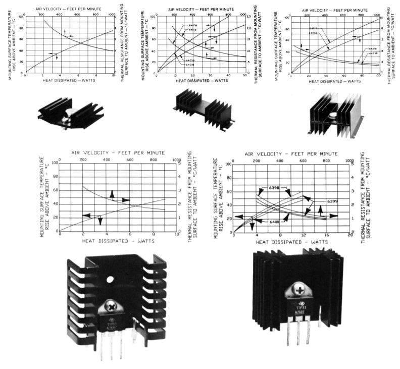
In order to increase the thermal efficiency of the device, an external heat sink is used. Heat sinks are normally made of aluminum and appear as a series of fins. The fins produce a large surface, which enhances the process of heat convection. In other words, the heat sink can transfer heat to the surrounding atmosphere faster than the power transistor can. By bolting the transistor to the heat sink, the device will be able to dissipate more power at a given operating temperature. Some typical heat sinks are shown in Figure 8.5.1 .
Physical Requirements
Heat sinks are designed to work with specific device-case styles. The most common case styles for regulators are the TO-220 “power tab”, and the TO-3 “can”. Heat sinks are available for these specific styles, including the requisite mounting hardware and insulation spacers. Some of the lower power regulators utilize TO-5 “mini can” or DIP-type cases. Heat sinks are available for these package types, too, but are not quite as common.
There are a couple of general rules that should be followed when using heat sinks:
- Always use some form of heat sink grease or thermally conductive pad between the heat sink and the device. This will increase the thermal transfer between the two parts. Note that excessive quantities of heat sink grease will actually decrease} performance.
- Mount fins in the vertical plane for optimum natural convective cooling.
- Do not overcrowd or obstruct devices that use heat sinks.
- Do not block air flow around heat sinks – particularly directly above and below items that rely on natural convection.
- If thermal demands are particularly high, consider using forced convection (e.g., fans).
Thermal Resistance
In order to specify a particular heat sink for a given application, a more technical explanation is in order. What we are going to do is create a thermal circuit equivalent. In this model, the concept of thermal resistance is used. Thermal resistance denotes how easy it is to transfer heat energy from one mechanical part to another. The symbol for thermal resistance is 𝜃 , and the units are Centigrade degrees per watt. In this model, temperature is analogous to voltage, and thermal power dissipation is analogous to current. A useful Equation is,
![\[P_D = \frac{\Delta T}{\theta _{total}} \]](https://pressbooks.nscc.ca/app/uploads/quicklatex/quicklatex.com-49131feb7a0dedadd5a767a743676b0a_l3.png "Rendered by QuickLaTeX.com")
(8.5.1)
Where 𝑃𝐷 is the power dissipated by the semiconductor device in watts, Δ𝑇 is the temperature differential, and 𝜃𝑡𝑜𝑡𝑎𝑙 is the sum of the thermal resistances. Basically, this is a thermal version of Ohm’s Law.
In order to construct our model, let’s take a closer look at the power-device/heat-sink combination. This is shown in Figure 8.5.2 . 𝑇𝑗 is the semiconductor junction temperature. This heat energy source heats the device case to 𝑇𝑐 . The thermal resistance between the two entities is 𝜃𝑗𝑐 . The case, in turn, heats the heat sink via the interconnection. This thermal resistance is 𝜃𝑐𝑠 , and the resulting temperature is 𝑇𝑠 .
Finally, the heat sink passes the thermal energy to the surrounding air, which is sitting at 𝑇𝑎 . The thermal resistance of the heat sink is 𝜃𝑠𝑎 . The equivalent thermal model is shown in Figure 8.5.3 . (Although this does not have perfect correspondence with normal circuit analysis, it does illustrate the main points.)
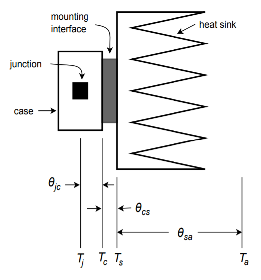

In this model, ground represents a temperature of absolute zero. The circuit is sitting at an ambient temperature 𝑇𝑎 , thus a voltage source of 𝑇𝑎 is connected to ground and the heat sink. The three thermal resistances are in series and are driven by a current source that is set by the present power dissipation of the device. Note that if the power dissipation is high, the resulting “voltage drops” across the thermal resistances are high. Voltage is analogous to temperature in this model, so this indicates that a high temperature is created. Because there is a maximum limit to 𝑇𝑗 , higher power dissipations require lower thermal resistances. As 𝜃𝑗𝑐 is set by the device manufacturer, you have no control over that element. However, 𝜃𝑐𝑠 is a function of the case style and the insulation material used, so you do have some control (but not a lot) over that. On the other hand, as the person who specifies the heat sink, you have a great deal of control over 𝜃𝑠𝑎 . Values for 𝜃𝑠𝑎 are given by heat sink manufacturers. A useful variation of Equation 8.5.1 is
![\[P_D = \frac{T_j-T_a}{\theta _{jc} + \theta _{cs} + \theta _{sa}} \]](https://pressbooks.nscc.ca/app/uploads/quicklatex/quicklatex.com-ca5c97aa47b8d581a4faadecd0eaafb8_l3.png "Rendered by QuickLaTeX.com")
(8.5.2)
Normally, power dissipation, junction and ambient temperatures, 𝜃𝑗𝑐 and 𝜃𝑐𝑠 are known. The idea is to determine an appropriate heat sink. Both 𝑇𝑗 and 𝜃𝑗𝑐 are given by the semiconductor device manufacturer. The ambient temperature, 𝑇𝑎 , may be determined experimentally. Due to localized warming, it tends to be higher than the actual “room temperature”. Standard graphs, such as those found in Figure 8.5.4 , may be used to determine 𝜃𝑐 .
Example 8.5.1
Determine the appropriate heat sink rating for a power device rated as follows: 𝑇𝑗(𝑚𝑎𝑥) = 150 ∘ C, TO-220 case style, 𝜃𝑗𝑐 = 3.0 C ∘ /W. The device will be dissipating a maximum of 6 W in an ambient temperature of 40 ∘ C. Assume that the heat sink will be mounted with heat sink grease and a 0.002 mica insulator.
First, find 𝜃𝑐𝑠 from the TO-220 graph. Curve 3 is used. The approximate (conservative) value is 1.6 C ∘ /W.
![\[P_D = \frac{T_j - T_a}{\theta _{jc} + \theta _{cs} + \theta _{sa}} \]](https://pressbooks.nscc.ca/app/uploads/quicklatex/quicklatex.com-880be12bb1edb4ae122ad58d19e40da3_l3.png "Rendered by QuickLaTeX.com")
![\[\theta _{sa} = \frac{T_j - T_a}{P_D} - \theta _{jc} - \theta _{cs} \]](https://pressbooks.nscc.ca/app/uploads/quicklatex/quicklatex.com-f5cf59d865e5679e78eb42a8c55fa20c_l3.png "Rendered by QuickLaTeX.com")
![\[\theta _{sa} = \frac{150^{\circ}C-40^{\circ}C}{6W} - 3.0C^{\circ}/W-1.6C^{\circ}/W \]](https://pressbooks.nscc.ca/app/uploads/quicklatex/quicklatex.com-4c65dbd794a8c0e0a85fd53cd4418909_l3.png "Rendered by QuickLaTeX.com")
![\[\theta _{sa} = 13.73C^{\circ}/W \]](https://pressbooks.nscc.ca/app/uploads/quicklatex/quicklatex.com-2e5093d8a689b751b751b2e6d8ca480c_l3.png "Rendered by QuickLaTeX.com")
This is the maximum acceptable value for the heat sink’s thermal resistance. Note that the use of heat sink grease gives us an extra 2 C ∘ /W or so. Also, note the generally lower values of 𝜃𝑠𝑎 for the TO-3 case relative to the TO-220. This is one reason why TO-3 cases are used for higher power devices. This case also makes it easier for the manufacturer to reduce 𝜃𝑗𝑐 .

