10.3 Single Supply Biasing
Up to this point, all of the example circuits have used a bipolar power supply, usually ± 15 V. Sometimes this is not practical. For example, a small amount of analog circuitry may be used along with a predominantly digital circuit that runs off a unipolar supply. It may not be economical to create an entire negative supply just to run one or two op amps. Although it is possible to buy op amps that have been specially designed to work with unipolar supplies1, the addition of simple bias circuitry will allow almost any op amp to run from a unipolar supply. This supply can be up to twice as large as the bipolar counterpart. In other words, a circuit that normally runs off a ± 15 V supply can be configured to run off of a +30 V unipolar supply, producing similar performance. We will look at examples using both the noninverting and inverting voltage amplifiers
The idea is to bias the input at one-half of the total supply potential. This can be done with a simple voltage divider. A coupling capacitor may be used to isolate this DC potential from the driving stage. For proper operation, the op amp’s output should also be sitting at one-half of the supply. This fact implies that the circuit gain must be unity. This may appear to be a very limiting factor, but in reality, it isn’t. The thing to remember is that the gain need only be unity for DC. The AC gain can be just about any gain you’d like.
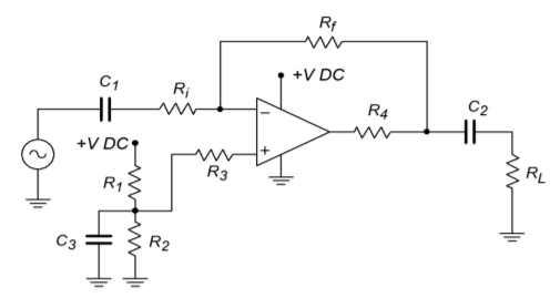
An example using the noninverting voltage amplifier is shown in Figure 4.3.1 . In order to set DC gain to unity without affecting the AC gain, capacitor 𝐶3 is placed in series with 𝑅𝑖 . 𝑅1 and 𝑅2 establish the 50% bias point. Their parallel combination sets the input impedance too. Resistors 𝑅3 and 𝑅4 are used to prevent destructive discharge of the coupling capacitors 𝐶1 and 𝐶2 into the op amp. They may not be required, but if present, typically run around 1 k Ω and 100 Ω respectively.
The inclusion of the capacitors produces three lead networks. A standard frequency analysis and circuit simplification shows that the approximate critical frequencies are
![\[f_{i n} = \frac{1}{2\pi C_1 R_1 || R_2} \]](https://pressbooks.nscc.ca/app/uploads/quicklatex/quicklatex.com-6ed545060bdf43b8ecdbe293b10e5ae8_l3.png "Rendered by QuickLaTeX.com")
![\[f_{out} = \frac{1}{2 \pi C_2 R_{load}} \]](https://pressbooks.nscc.ca/app/uploads/quicklatex/quicklatex.com-0647625ca87041ad57570c70b2a2199e_l3.png "Rendered by QuickLaTeX.com")
![\[f_{fdbk} = \frac{1}{2\pi C_3 R_i} \]](https://pressbooks.nscc.ca/app/uploads/quicklatex/quicklatex.com-b6da52b351086be850b86cdc9931b005_l3.png "Rendered by QuickLaTeX.com")
The input bias network can be improved by using the circuit of Figure 4.3.2 . This reduces the hum and noise transmitted from the power supply into the op amp’s input. It does so by creating a low impedance at node A. This, of course, does not affect the DC potential. 𝑅5 now sets the input impedance of the circuit.

The important points to remember here are that voltage gain is still 1+𝑅𝑓/𝑅𝑖 in the midband, 𝑍𝑖𝑛 is now set by the biasing resistors 𝑅1 and 𝑅2 , or 𝑅5 (if used), and that frequency response is no longer flat down to zero Hertz.
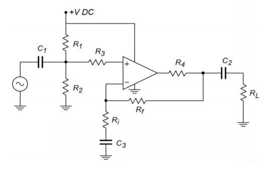
A single-supply version of the inverting voltage amplifier is shown in Figure 4.3.3 . It uses the same basic techniques as the noninverting form. The bias setup uses the optimized low-noise form. Note that there is no change in input impedance, it is still set by 𝑅𝑖 . The approximate lead network critical frequencies are found through
![\[f_{in} = \frac{1}{2\pi C_1 R_i} \]](https://pressbooks.nscc.ca/app/uploads/quicklatex/quicklatex.com-a5008763fc21e6cc25747e3f6e1d29a2_l3.png "Rendered by QuickLaTeX.com")
![\[f_{out} = \frac{1}{2\pi C_2 R_{load}} \]](https://pressbooks.nscc.ca/app/uploads/quicklatex/quicklatex.com-e4703c5bb2168cf979ccd313a17a91aa_l3.png "Rendered by QuickLaTeX.com")
![\[f_{bias} = \frac{1}{2\pi C_3 R_1 || R_2} \]](https://pressbooks.nscc.ca/app/uploads/quicklatex/quicklatex.com-48c19ffe6799cdba52ba4fa94d3160d4_l3.png "Rendered by QuickLaTeX.com")
Note the general similarity between the circuits of Figures 4.3.3 and 4.3.1 . A simple redirection of the input signal creates one form from the other.