
3.4 The E-MOSFET
The E-MOSFET is available in both low power and high power versions. It operates in enhancement mode (first quadrant) only. The construction of the low power version is similar to that of the DE-MOSFET but with one important distinction. A simplified cross-section of an N-channel E-MOSFET is shown in Figure 3.4.1 .
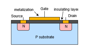
In the E-MOSFET, the P material extends up through the channel and to the gate insulating layer. This has the effect of preventing current flow with negative gatesource voltages applied. Consequently, E-MOSFETs are sometimes referred to as normally off devices. In fact, the E-MOSFET will not conduct if 𝑉𝐺𝑆 is zero, or even for small positive values of 𝑉𝐺𝑆. The P and N materials functionally create energy hills or barriers that prevent current flow through the channel. This can be compared to an NPN BJT that has an open base terminal: no collector current would flow (unless the collector-emitter voltage exceeded the breakdown limit).
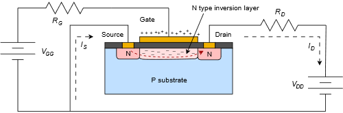
To understand how the E-MOSFET functions, refer to Figure 3.4.2 . This diagram shows the device with positive drain and gate supplies attached to it through limiting resistors. The dashed lines indicate electron current flow. As with the DE-MOSFET, the gate can be seen as one plate of a capacitor while the P material serves as the other plate. A positive voltage on the gate will lead to a negative charge on the P material side. If the charge is large enough, all of the holes in the P material can be filled leaving the portion of the material situated near the isolation layer neutral (neither P nor N). Any further increase in gate voltage injects more negative charge into this region, this making it behave like N material. This is called an N-type inversion layer and it allows a path for current to flow. The more positive we make the gate voltage, the greater the effect, and the greater the current.
The voltage where the current begins to flow is called the threshold voltage and is usually denoted as 𝑉𝐺𝑆(𝑡ℎ), although it is sometimes shortened to 𝑉𝑡ℎ or just 𝑉𝑡 . Like both the JFET and DE-MOSFET, the E-MOSFET drain curve family exhibits three characteristic regions: the ohmic or triode region, the constant current or saturation region, and the breakdown region.
The characteristic equation for the E-MOSFET operating in its constant current region is given below. Like the other FETs examined, this is a square-law device.
![\[I_D = k (V_{GS}-V_{GS (th)} )^2 \]](https://pressbooks.nscc.ca/app/uploads/quicklatex/quicklatex.com-fae6952d9ef920ec502c7a1ff4c2a832_l3.png "Rendered by QuickLaTeX.com")
(3.4.1)
Where
𝐼𝐷 is the drain current,
𝑉𝐺𝑆 is the gate-source voltage (𝑉𝐺𝑆(𝑡ℎ)≤𝑉𝐺𝑆≤𝐵𝑉𝐺𝑆),
𝑉𝐺𝑆(𝑡ℎ) is the the threshold voltage,
𝑘 is a device parameter (a constant, units of amps/volt 2 or siemens/volt).
The derivative of Equation 3.4.1 yields the transconductance.
![\[g_m = \frac{d I_D}{d V_{GS}} = 2k (V_{GS} -V_{GS(th)} ) \]](https://pressbooks.nscc.ca/app/uploads/quicklatex/quicklatex.com-10852903a1c8ab0ed10ddbf10ae5e167_l3.png "Rendered by QuickLaTeX.com")
(3.4.2)
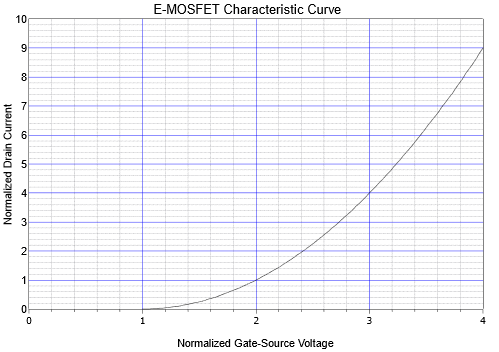
Equation 3.4.1 is plotted in Figure 3.4.3 . The normalized gate-source voltage is 𝑉𝐺𝑆/𝑉𝐺𝑆(𝑡ℎ) and the normalized drain current is the ratio of 𝐼𝐷 to the current generated when 𝑉𝐺𝑆 is twice 𝑉𝐺𝑆(𝑡ℎ). This curve is reminiscent of the characteristic curve of a BJT. First, they are both in the first quadrant. Second, both curves exhibit an increasing positive slope. Finally, the curves don’t begin to “take off” until some specific turn-on voltage is reached. In the case of the BJT, that voltage is approximately 0.7 V for a silicon device. For the E-MOSFET, that voltage is 𝑉𝐺𝑆(𝑡ℎ). Obviously though, the MOSFET curve does not increase as rapidly as the BJT curve.
The power E-MOSFET utilizes a different construction from low power MOSFETs and offers certain advantages over power BJTs including very fast switching speed and lower drive current demands. Consequently, they tend to be favored over BJTs in high power, high speed switching applications such as switching power supply regulators, DC-to-DC converters and class D amplifiers (Chapter 14). These devices also exhibit extremely low 𝑟𝐷𝑆(𝑜𝑛) values, in some cases just a few milliohms. There are different methods of construction, the most recent being the trench style. A cutaway view is shown in Figure 3.4.4 .
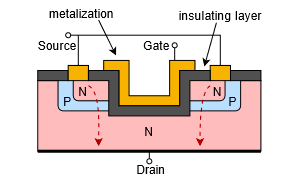
A power E-MOSFET is made of a large number of cells, each featuring the U-shaped gate “trench” (an earlier style used a V-shaped trench). Note the location of the drain, now opposite of the gate and source. The advantage here is that the current flows vertically rather than laterally. This results in a much lower 𝑟𝐷𝑆(𝑜𝑛) and considerably greater current capacity. The characteristic curve still echoes that of Figure 3.4.3 although it tends to be steeper when compared to low power devices.
