
2.6 Ohmic Region Operation
As noted in the previous chapter, the JFET’s operational curves span three regions. Two have been discussed: the constant current region is where the normal amplifiers and followers are biased, and breakdown is a region to be avoided due to potential damage. The third region is known as the ohmic region, or triode region. It occurs in the area where 𝑉𝐷𝑆 is less than the pinch-off voltage, 𝑉𝑃. In this area, the device behaves more like a resistor than like a current source. If we were to examine a family of drain curves, like those of Figure 1.2.3, and magnify the area near the origin, we would see something like the plot in Figure 2.6.1 .

If 𝑉𝐷𝑆 is a small value, typically less than 100 mV or so, each of the curves appears as a straight line. Further, the slope of that line is a function of the gate-source voltage, 𝑉𝐺𝑆. The closer 𝑉𝐺𝑆 is to 0 V, the steeper the slope (violet line) and the closer 𝑉𝐺𝑆 is to 𝑉𝐺𝑆(𝑜𝑓𝑓), the more shallow the slope (dark red line). Finally, if 𝑉𝐺𝑆=𝑉𝐺𝑆(𝑜𝑓𝑓) the slope is nearly zero (aqua line). Because this is a plot of drain current versus drain-source voltage, the slope indicates the conductance of the channel. In somewhat more useful terms, we can say that the reciprocal of the slope indicates the resistance of the channel. Therefore, if 𝑉𝐺𝑆=0 V, the channel resistance will be at its minimum, and when 𝑉𝐺𝑆=𝑉𝐺𝑆(𝑜𝑓𝑓), the channel resistance will be at its maximum. The maximum channel resistance can be quite high, well into the hundreds of kilo-ohms. The minimum channel resistance varies considerably from device to device. It is found on a data sheet as 𝑟𝐷𝑆(𝑜𝑛). 𝑟𝐷𝑆(𝑜𝑛) can be as small as a few ohms for specialized JFETs and as large as hundreds of ohms for general purpose devices.[1] For example, the data sheet for the J111 series JFETs found in Figure 10.3.1 shows maximum values of 30 Ω , 50 Ω and 100 Ω for the J111, J112 and J113, respectively. The channel resistance does not follow a linear relation with 𝑉𝐺𝑆.
To be more specific, in this region the drain current no longer follows the characteristic equation we used for biasing (Equation 1.2.1). The drain current equation in the ohmic region is:
![\[I_D = \frac{V_{DS}}{V_P} 2 I_{DSS} \left( \left( 1 - \frac{V_{GS}}{V_P} \right) - \frac{V_{DS}}{V_P} \right) \]](https://pressbooks.nscc.ca/app/uploads/quicklatex/quicklatex.com-df7ccb9bba9846c380fdfc472fe225d7_l3.png "Rendered by QuickLaTeX.com")
(2.6.1)
Where 𝑉𝑃=|𝑉𝐺𝑆(𝑜𝑓𝑓)| and 𝑉𝐺𝑆 is to be taken as an absolute value and lies between 0 and 𝑉𝑃.
Recalling that, in general, 𝑟𝐷𝑆=𝑉𝐷𝑆/𝐼𝐷, we can substitute Equation 2.6.1 for 𝐼𝐷 and, after including the definition of 𝑔𝑚0, arrive at an expression for 𝑟𝐷𝑆:
*** QuickLaTeX cannot compile formula:
\[r_{DS} = \frac{V_P}{g_{m0} \left( V_P -V_{GS} - \frac{V_{DS}}{2} \right) \]

*** Error message:
File ended while scanning use of \frac .
Emergency stop.
For small values of 𝑉𝐷𝑆, this reduces to a simple equation:
![\[r_{DS} = \frac{V_P}{g_{m0} (V_P -V_{GS} )} \]](https://pressbooks.nscc.ca/app/uploads/quicklatex/quicklatex.com-62d4669877daa20739792fe1442b14f1_l3.png "Rendered by QuickLaTeX.com")
(2.6.2)
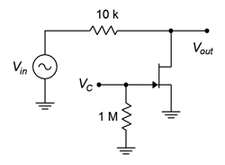
What we have created here is voltage-controlled resistor. Equation 2.6.2 shows that the resistance of the channel is a function of the gate-source voltage: the channel resistance will be at its minimum (𝑟𝐷𝑆(𝑜𝑛)) when 𝑉𝐺𝑆=0 V, and it approaches infinity when 𝑉𝐺𝑆 equals 𝑉𝐺𝑆(𝑜𝑓𝑓). Generally, there are two applications that make use of the ohmic region: an electronic rheostat/potentiometer and an analog switch. A simple circuit that can be used for either application is shown in Figure 2.6.2.

Note that no external bias is applied to the circuit. Instead, a control voltage, 𝑉𝐶, is applied to the gate and the input signal is applied to a resistor attached to the drain terminal. The output is taken across the JFET’s drain-source.
The idea behind this circuit is the basic resistive voltage divider. The JFET’s channel resistance, 𝑟𝐷𝑆, forms a voltage divider along with 𝑅𝐷.
![\[v_{out} = V_{i n} \frac{r_{DS}}{r_{DS}+R_D} \]](https://pressbooks.nscc.ca/app/uploads/quicklatex/quicklatex.com-9996702e8045478cf8025324fb2b9488_l3.png "Rendered by QuickLaTeX.com")
If 𝑟𝐷𝑆≫𝑅𝐷, 𝑣𝑜𝑢𝑡 approaches 𝑣𝑖𝑛. Conversely, if 𝑟𝐷𝑆≪𝑅𝐷, 𝑣𝑜𝑢𝑡 approaches zero. Normally, 𝑅𝐷 is set somewhere between the maximum and minimum channel resistances in order to obtain the widest range of operation.
As the control voltage 𝑉𝐶 is 𝑉𝐺𝑆, then 𝑉𝐶 controls the size of 𝑣𝑜𝑢𝑡. If we set 𝑉𝐶 to 0 V, 𝑟𝐷𝑆 is very small and thus 𝑣𝑜𝑢𝑡≈0 . On the other hand, if 𝑉𝐶 is set to a large negative potential (beyond 𝑉𝐺𝑆(𝑜𝑓𝑓) ), then 𝑣𝑜𝑢𝑡≈𝑉𝑖𝑛. If 𝑉𝐶 is set between these extremes then 𝑣𝑜𝑢𝑡 will be somewhere in the middle range. If 𝑉𝐶 is continuously variable, then the circuit behaves like a solid-state potentiometer. If, in contrast, 𝑉𝐶 is only set at the limits, then the circuit behaves like a switch, either allowing or preventing the signal from transferring through. This is known as an analog switch.
A single JFET/resistor combination as shown in Figure 2.6.2 will have limited isolation as an analog switch and only a modest range of adjustment when used as a voltage-controlled potentiometer. To improve performance, multiple circuits can be cascaded or other JFETs can be added to create a “pi” attenuator network.
This voltage-controlled resistor has a huge advantage over traditional electromechanical potentiometers and switches: speed. In this circuit, the resistance can be changed at very high rates, essentially, as fast as 𝑉𝐶 can change. Consequently, it would be no big deal to switch the input signal on and off at rates well over 100,000 times per second. No mechanical switch or potentiometer can hope to perform anywhere near that speed, and any attempt to do so would lead to the devices burning up from the friction. In general, flaming potentiometers are frowned upon during the design and development process, although it would make a decent name for an indie rock band. Another advantage is that a switch can be thrown “remotely”, that is, we only need to route the control voltage to the switch operator, not the signal itself. This can reduce system noise. It’s also easier to implement if the switch is being “thrown” programmatically, such as via a microcontroller.
Example 2.6.1
For the circuit shown in Figure 2.6.3 , if the input signal is 50 mV, determine the output voltage for 𝑉𝐶=0 VDC and −6 VDC. Assume 𝑉𝐺𝑆(𝑜𝑓𝑓)=−5 V, 𝑟𝐷𝑆(𝑜𝑛)=30 Ω and 𝑟𝐷𝑆(𝑜𝑓𝑓)=800 k Ω .
For 𝑉𝐶=0 VDC, the channel resistance will be at its minimum of 𝑟𝐷𝑆(𝑜𝑛).
![\[V_{out} = V_{i n} \frac{r_{DS (on)}}{R_D+r_{DS (on )}} \]](https://pressbooks.nscc.ca/app/uploads/quicklatex/quicklatex.com-bcf72ae9cfb2112cee91d781ca71c122_l3.png "Rendered by QuickLaTeX.com")
![\[V_{out} = 50mV \frac{30\Omega}{10 k \Omega +30\Omega} \]](https://pressbooks.nscc.ca/app/uploads/quicklatex/quicklatex.com-a0500607c4ca1ed2c9498db913f2a03a_l3.png "Rendered by QuickLaTeX.com")
![\[V_{out} = 0.15 mV \]](https://pressbooks.nscc.ca/app/uploads/quicklatex/quicklatex.com-a8fa5bdc5c052d2115b20aa119e27479_l3.png "Rendered by QuickLaTeX.com")
The signal has been reduced by a factor of over 330. That’s not as good as a mechanical switch but if we cascaded two of these the overall reduction would be more than 100,000:1.
For 𝑉𝐶=−6 VDC, the channel resistance will be at its maximum of 𝑟𝐷𝑆(𝑜𝑓𝑓).
*** QuickLaTeX cannot compile formula:
\[V_{out} = V_{i n} \frac{r_{DS (off )}{R_D+r_{DS (off )}}  \]

*** Error message:
File ended while scanning use of \frac .
Emergency stop.
![\[V_{out} = 50 mV \frac{800 k\Omega}{10k \Omega +800 k \Omega} \]](https://pressbooks.nscc.ca/app/uploads/quicklatex/quicklatex.com-e534429898d34f0b05af981eb6f33850_l3.png "Rendered by QuickLaTeX.com")
![\[V_{out} = 49.4mV \]](https://pressbooks.nscc.ca/app/uploads/quicklatex/quicklatex.com-ab62ed7d1e06dfa67a9290d916f19d00_l3.png "Rendered by QuickLaTeX.com")
This represents nearly 99% of the input signal, so the signal is passed through cleanly.
Computer Simulation
To verify the results of the preceding example, the circuit is entered into a simulator as shown in Figure 2.6.4 . A J111 JFET model is used which has parameters similar to those used in the example.

A transient analysis is run twice; the first time is with a control voltage of 0 V and the second with a control voltage of −6 V. In the first case, the output should be just a small residual and in the second, we should see the full input signal. The results of the first trial are shown in Figure 2.6.5 while the second is shown in Figure 2.6.6 .
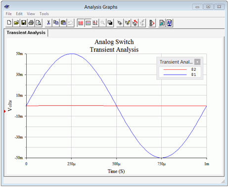
With 𝑉𝐶 at 0 V, the output trace (red, at node 2) is nearly flat. The precise value of its peak is 0.167 mV, not far from the value calculated in Example 2.6.1.
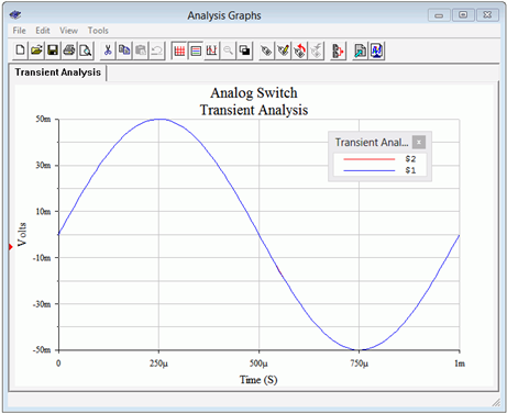
In contrast, when 𝑉𝐶=−6 V the JFET is off, offering a high impedance and no loss of signal. At first glance, it may appears as though the output trace is missing but what has happened is that it is hidden behind the input trace (blue, node 1). The amplitudes are virtually identical so the blue trace completely obscures the red trace.
- 𝑟𝐷𝑆(𝑜𝑛) can be as little as a few milliohms for specialized high power MOSFETs (Chapters 12 and 13). ↵
