
2.5 Multi-stage and Combination Circuits
The rules for multi-stage circuits utilizing JFETs are the same as those discussed for BJTs: Steps must be taken to ensure that the bias of one stage does not adversely affect the bias of surrounding stages (typically by using coupling capacitors or going to a DC coupled system), the load for a given stage will be the input impedance of the following stage, the input impedance of the system will be the input impedance of the first stage, and the system gain will be the product of the individual stage gains.
Keeping those items in mind, there are no limits concerning mixing BJTs with JFETs, or mixing N-channel with P-channel devices. There are certain practical issues, however, that might dictate where certain devices are used. JFETs, due to their high input impedance and modest gain potential, tend to be used at the front end of amplifying systems. Their comparatively low self-noise is also a bonus at this location. BJTs, on the other hand, have high gain potential and tend to be used in the remaining stages. Their high distortion can be tamed through swamping.
To examine the possibilities, let’s walk through the mixed, multi-stage amplifier presented in Figure 2.5.1 .
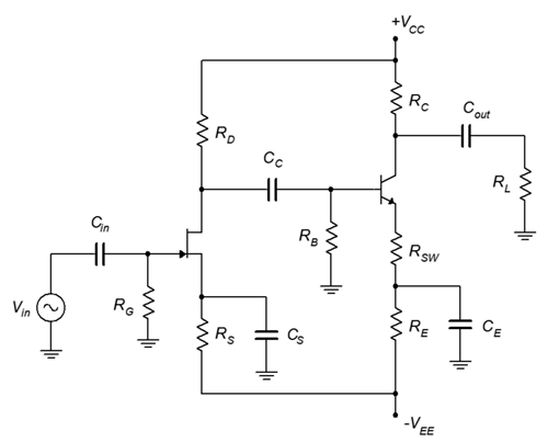
his amplifier uses a bipolar power supply which gives the designer a lot of flexibility. The first stage consists of a JFET common source amplifier. It utilizes combination bias (notice that 𝑅𝑆 is connected to the shared negative supply, 𝑉𝐸𝐸, that also serves as 𝑉𝑆𝑆). 𝐶𝑆 bypasses the source resistor so this stage does not use swamping. Distortion should not be an issue unless the input signal is fairly large. The load for this stage is 𝑅𝐷 in parallel with the input impedance to the second stage (coupling capacitor 𝐶𝐶 will appear ideally as a short for signal frequencies).
The second stage utilizes an NPN BJT configured as a swamped common emitter amplifier. It utilizes two-supply emitter bias. It’s input impedance is the parallel combination of 𝑅𝐵 and 𝑍𝑖𝑛(𝑏𝑎𝑠𝑒) . The base input impedance, in turn, is a function of 𝛽 and 𝑅𝑆𝑊 ( 𝑟′𝑒 will have only a small impact due to the swamping resistor). The load for this stage will be 𝑅𝐿 in parallel with 𝑅𝐶. That value divided by 𝑅𝑆𝑊 will give the approximate stage gain (again, 𝑟′𝑒 will have little impact). Although the second stage will be dealing with a larger signal, distortion will be mitigated by the swamping resistor.
The system gain will be the product of the two stage gains. As they both invert the signal, the inversion of the inversion will lead to an output signal that is in phase with the input signal. The system input impedance will depend on the JFET first stage and can be approximated to be equal to 𝑅𝐺, at least at low frequencies.
