9.4 The Four Variants of Negative Feedback
Negative feedback can be achieved via four different forms. They differ in how the input and output impedances are changed. We have basically two choices when it comes to connecting the input and output of the amplifier to the output and input of the feedback network. We may produce either a series connection or a parallel connection. This yields four possibilities total. Each connection will produce a specific effect on the input or output impedance of the system. As you might guess, parallel connections decrease the impedance and series connections increase it. A high input impedance is desirable for maximum voltage transfer, whereas a low impedance is required for maximum current transfer. As a memory aid, think of volt meters and ammeters. For the smallest loading effect, volt meters should exhibit a high impedance and ammeters a very low one. In the case of the output connection, a low source impedance is required for the best voltage transfer, and a high source impedance for current transfer. You should think of the ideal voltage source (zero 𝑍𝑜𝑢𝑡 ) and the ideal current source (infinite 𝑍𝑜𝑢𝑡 ) here. Consequently, if we were to connect our feedback network in series with the amplifier’s input, and in parallel with its output, we would have an increase in 𝑍𝑖𝑛 and a decrease in 𝑍𝑜𝑢𝑡 . This means that our system would be very good at sensing an input voltage, and ideal for producing a voltage. We will have created a voltage-controlled voltage source (VCVS), the ideal voltage amplifier. So that you can get a good idea of the possibilities, all four types are summarized in the following table.
| Type (in-out) | 𝑍𝑖𝑛 | 𝑍𝑜𝑢𝑡 | Model | Idealization | Transfer Ratio |
|---|---|---|---|---|---|
| Series-Parallel | High | Low | VCVS | Voltage Amplifier | 𝑉𝑜𝑢𝑡/𝑉𝑖𝑛 Voltage gain |
| Series-Series | High | High | VCCS | Voltage to Current Transducer | 𝐼𝑜𝑢𝑡/𝑉𝑖𝑛 Transconductance |
| Parallel-Parallel | Low | Low | CCVS | Current to Voltage Transducer | 𝑉𝑜𝑢𝑡/𝐼𝑖𝑛 Transresistance |
| Parallel-Series | Low | High | CCCS | Current Amplifier | 𝐼𝑜𝑢𝑡/𝐼𝑖𝑛 Current Gain |
Table 9.4.1
Generally speaking, the input and output impedances will be raised or lowered from the non-feedback value by the sacrifice factor. Note that by using the proper form of feedback, we can achieve any of the possible models. This greatly enhances our ability to deal with specific applications. Much work in our field relies on optimal voltage transfer, therefore Series-Parallel (SP) is often used. A variation on Parallel Parallel (PP) is also used frequently, as we shall see.
Series-Parallel (SP)
The SP connection makes for the ideal voltage amplifier. A generalized block diagram is shown in Figure 3.4.1 . You can tell that it has a series input because there is no input current node. Contrast this with the output: Note that the op amp’s output current splits into two paths, one through the load and the other into the feedback network. This output node clearly denotes the feedback’s parallel output connection.
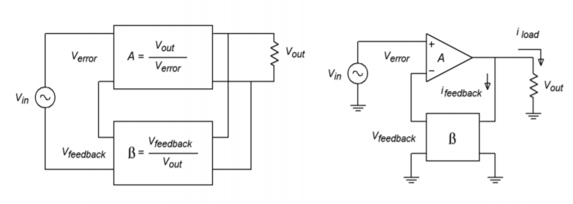
Let’s take a look at exactly how SP negative feedback alters the system gain, impedances, and frequency response. For starters, let’s examine the closed-loop gain ( 𝐴𝑠𝑝 ). Our amplifier block produces a gain 𝐴 , and could be a diff amp, op amp, or other multi-stage possibility. The feedback network is typically a voltage divider and produces a loss, 𝛽 . The signal presented to the inverting input of the amp is the feedback signal and is equal to 𝑉𝑜𝑢𝑡𝛽 . Note that the source’s signal, 𝑉𝑖𝑛, is applied to the non inverting input. Therefore, the differential input voltage (usually referred to as 𝑉𝑒𝑟𝑟𝑜𝑟 ), equals 𝑉𝑖𝑛–𝑉𝑓𝑒𝑒𝑑𝑏𝑎𝑐𝑘 . We also know from previous work with differential amplifiers that that 𝑉𝑜𝑢𝑡=𝑉𝑒𝑟𝑟𝑜𝑟𝐴𝑜𝑙 ( 𝐴𝑜𝑙 is the amplifiers open-loop gain). In other words we know:
![]()
(9.4.1)
![]()
(9.4.2)
![]()
(9.4.3)
and by definition,
![]()
(9.4.4)
Substituting Equation 3.4.3 into Equation 3.4.2 ,
![]()
(9.4.5)
Substituting Equation 3.4.5 into Equation 3.4.1 , and simplifying,
![]()
(9.4.6)
Finally, substituting Equation 3.4.6 and Equation 3.4.3 into Equation 3.4.4 and simplifying, yields,
![]()
(3.4.7)
Since the fundamental definition of sacrifice factor, 𝑆 , is 𝐴𝑜𝑙/𝐴𝑐𝑙 , we may also say 𝐴𝑠𝑝=𝐴𝑜𝑙/𝑆 and therefore, for SP,
![]()
(3.4.8)
Equation 3.4.7 is our general gain Equation but, if we can make 𝛽𝐴𝑜𝑙≫1 we may ignore the “+1” in the denominator and further simplify this as,
![]()
(9.4.9)
This seemingly innocent Equation packs a rather hefty punch. What it is telling us is that the open-loop gain of the amplifier does not} play a role in setting the system gain, as long as the open-loop gain is very large. In other words, the system gain is controlled solely by the feedback network. Consequently, our amplifier can exhibit large gain changes in its open-loop response, but the closed-loop response will remain essentially constant. For this reason we will achieve identical closed-loop gains for op amps that exhibit sizable differences in their open-loop gains. Because signal distortion is produced by non-linearities that can be viewed as dynamic gain changes, our closed-loop distortion drops as well. Also, it is this very effect that extends our closed-loop frequency response. Imagine that our amplifier exhibits a gain of 10,000 at its upper break frequency of 100 Hz. If the feedback factor is equal to 0.1, our exact gain is:
![]()
If we were to measure the amplifier’s open-loop gain one decade up, at 1 kHz, it should be around 1,000 (assuming 20 dB/decade loss). The closed loop gain now equals:
![]()
As you can see, the closed-loop gain changed only about 1 despite the fact that the open-loop gain dropped by a factor of 10. If we continue to raise the frequency, Asp would equal 9.09 at 10 kHz. Finally, at 100 kHz a sizable drop is seen because the gain falls to 5. At this point, our assumption of 𝛽𝐴𝑜𝑙>>1 falls apart. Note however, that our loss relative to the midband gain is only a few dB. We have effectively stretched out the bandwidth of the system. Actually, this calculation is somewhat over-simplified as we have ignored the extra phase lag produced by the amplifier above the open-loop break frequency. If we assume that the open-loop response is dominated by a single lag network (and it should be, in order to guarantee stability, remember?), a phase sensitive version of Equation 3.4.7 would be:
![]()
This extra phase will reach its maximum of -90 degrees approximately one decade above the open-loop break frequency. Consequently, when we find the magnitude of gain at 100 kHz, it’s not
![]()
but rather
![]()
which equals 7.07, for a -3 dB relative loss
A simpler way of stating all of this is: The new upper break frequency is equal to the open-loop upper break times the sacrifice factor, 𝑆 . Because 𝑆 is the loop gain, it is equal to 𝐴𝑜𝑙/𝐴𝑠𝑝 . Note that our low frequency 𝑆 = 10,000/10, or 1,000. Therefore, our closed-loop break equals 1,000 times 100 Hz, or 100 kHz. A very important item to notice here is that there is an inverse relation between closed-loop gain and frequency response. Systems with low gains will have high upper-breaks, while high gain systems will suffer from low upper-breaks. This sort of trade-off is very common. Although most diff amps and op amps do not have lower break frequencies, circuits that do will see an extension of their lower response in a similar manner. (i.e., the lower break will be reduced by 𝑆 ). In order to achieve both high gain and wide bandwidth, it may be necessary to cascade multiple low gain stages.
Example 9.4.1
Assume that you have an amplifier connected as in Figure 3.4.1 . The open loop gain ( 𝐴𝑜𝑙 ) of the amp is 200 and its open loop upper break frequency ( 𝑓2−𝑜𝑙 ) is 10 kHz. If the feedback factor ( 𝛽 ) is 0.04, what are the closed loop gain ( 𝐴𝑠𝑝 ) and break frequency ( 𝑓2−𝑠𝑝 )
For 𝐴𝑠𝑝 ,
![]()
![]()
![]()
The approximation says,
![]()
![]()
![]()
That is reasonably close to the general equation’s answer (note that there is no need to include phase effects as we are looking for the midband gain). The approximation is more accurate when 𝐴𝑜𝑙 is larger.
For 𝑓2−𝑠𝑝 , first find the sacrifice factor, 𝑆
![]()
![]()
![]()
![]()
![]()
![]()
One interesting thing to note is that the product of the gain and upper break frequency will always equal a constant value, assuming a 20 dB per decade roll off. Our open loop product is 200 times 10 kHz, or 2 MHz. Our closed loop product is 22.22 times 90 kHz, which is 2 MHz. If we choose any other feedback factor, the resulting 𝐴𝑠𝑝 and 𝑓2−𝑠𝑝 will also produce a product of 2 MHz (try it and see). The reason for this is simple. A 20 dB per decade rolloff means that the gain drops by a factor of 10 when the frequency is increased by a factor of 10. There is a perfect 1:1 inverse relationship between the two parameters. No matter how much you increase one parameter, the other one will decrease by the same proportion. Thus, the product is a constant.
At this point you may be asking yourself, “What exactly is in that feedback network and how do I figure out 𝛽 ?” Usually, the feedback network just needs to produce a loss – it has to scale 𝑉𝑜𝑢𝑡down to 𝑉𝑓𝑒𝑒𝑑𝑏𝑎𝑐𝑘 . The simplest item for the job would be a resistive voltage divider. (It is possible to have complex frequency dependent or non-linear elements in the network as we shall see in the future). An example is presented in Figure 3.4.2 . If you study this diagram for a moment, you will notice that the feedback factor 𝛽 is really nothing more than the voltage divider loss. 𝑉𝑜𝑢𝑡is the input to the feedback network and appears across 𝑅𝑓+𝑅𝑖||𝑍𝑖𝑛 . The output of the network is 𝑉𝑓𝑒𝑒𝑑𝑏𝑎𝑐𝑘 , which appears across 𝑅𝑖 . Simply put, the ratio is
![]()
If the 𝑍𝑖𝑛 is large enough to ignore, as in most op amps, this simplifies to
![]()
By substituting this Equation into our approximate gain Equation 3.4.9 , we find
![]()
(9.4.10)
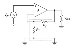
Note that the values of 𝑅𝑓 and 𝑅𝑖 are not really important, rather, their ratio is. We would arrive at the same gain if 𝑅𝑓=10𝑘Ω and 𝑅𝑖=1𝑘Ω , or 𝑅𝑓=20𝑘Ω and 𝑅𝑖=2𝑘Ω . We obviously have quite a bit of latitude when designing circuits for a specific gain, but we do face a few practical limits. If the resistors are too small we will run into problems with op amp output current. On the other hand, if the resistors are too large, excessive noise, offset, drift and loading effects will result. As a guideline for general-purpose circuits, 𝑅𝑓+𝑅𝑖 is usually in the range of 10 k to 100 k Ω .
Computer Simulation
As evidenced earlier, if the open loop gain is very high, its precise value does not matter. We’ll examine this effect using Example 3.4.1 , but with much higher open loop gains. The simulation is shown in Figure 3.4.3 using Multisim and the basic op amp model presented in Chapter Two. The circuit uses 𝑅𝑓=24𝑘Ω and 𝑅𝑖=1𝑘Ω for an ideal closed loop voltage gain of 25. The input signal is set to 40 millivolts.

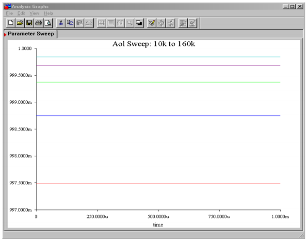
Using the Parameter Sweep option, the open loop gain is initialized at 10,000 and is progressively doubled to a maximum of 160,000. These are reasonable gain values for a production op amp. The output transient analysis shows that in spite of a 16 to 1 variation in open loop gain, all output voltages are approximately 1 V, achieving a closed loop gain of nearly 25 in all cases.
Example 9.4.2
Let’s say that the microphone that you use for acoustic instruments produces a signal that is just too weak for you to record without excessive noise. After a little experimentation in lab, you discover that you need about 20 dB of voltage gain before you can successfully capture a softly picked guitar. Using Figure 3.4.4 as a guide, design this amplifier with the following device: 𝐴𝑜𝑙 = 50,000, 𝑍𝑖𝑛−𝑜𝑙=600𝑘Ω .
First, note that our 𝐴𝑜𝑙 and 𝑍𝑖𝑛−𝑜𝑙 values are more than sufficient for us to use the approximation formulas. Because our formulas all deal with ordinary gain, we must convert 20 dB.
![]()
![]()
![]()
By rearranging Equation 3.4.10 ,
![]()
![]()
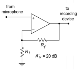
We see that 𝑅𝑓 must be 9 times larger than 𝑅𝑖 . There is no single right answer here; there are many possibilities.
Computer Simulation
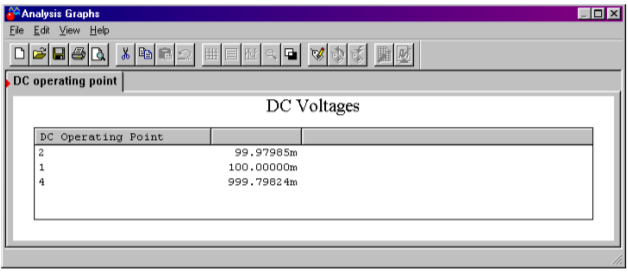
One viable solution for Example 3.4.2 is simulated using Multisim in Figure 3.4.5 . This circuit uses 𝑅𝑓=9𝑘Ω and 𝑅𝑖=1𝑘Ω . The op amp model is the simple dependent source version examined in Chapter Two. The input signal is set to 0.1 V DC for simplicity. Both the output and feedback potentials are presented. The results of this simulation verify our hand calculations. In order to note the sensitivity of the design, you can alter certain parameters of the input file and rerun the simulation. Two of the more interesting areas are the absolute values of the feedback resistors and the open loop gain of the op amp. You will note that as these quantities are lowered, our approximation formulas become less accurate. With the given values, the approximations deviate from the simulation results by less than 1.

SP Impedance Effects
As noted earlier, negative feedback affects the closed-loop input and output impedances of our system. Series connections increase the impedance and parallel connections decrease the impedance.
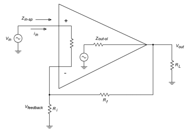
Let’s see exactly how this works in the SP case. First, we must distinguish between the 𝑍𝑖𝑛 of the amplifier itself and the 𝑍𝑖𝑛 of the system with feedback. We shall call them 𝑍𝑖𝑛−𝑜𝑙 and 𝑍𝑖𝑛−𝑠𝑝 respectively. Figure 3.4.6 shows this difference by using a simple model of the amplifier. By definition,
![]()
The idea here is to notice that the source only needs to supply enough signal current to develop the 𝑉𝑒𝑟𝑟𝑜𝑟 drop across the amplifier’s 𝑍𝑖𝑛−𝑜𝑙 . As far as the 𝑉𝑖𝑛signal source is concerned, 𝑉𝑓𝑒𝑒𝑑𝑏𝑎𝑐𝑘 is a voltage source, not a voltage drop. Therefore, 𝐼𝑖𝑛=𝑉𝑒𝑟𝑟𝑜𝑟/𝑍𝑖𝑛−𝑜𝑙 .
We may now say,
![Rendered by QuickLaTeX.com \[Z_{in -sp} = \frac{V_{in}}{\left(\frac{V_{error}}{Z_{in-ol}}\right)} = \frac{Z_{in-ol}V_{in}}{V_{error}} \]](https://pressbooks.nscc.ca/app/uploads/quicklatex/quicklatex.com-e7a33c842343c984990488c73783b97e_l3.png)
Because 𝑉𝑒𝑟𝑟𝑜𝑟 ideally equals 𝑉𝑜𝑢𝑡/𝐴𝑜𝑙
![]()
Sacrifice factor 𝑆 , is defined as 𝐴𝑜𝑙/𝐴𝑠𝑝 , so,
![]()
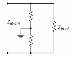
This is our ideal SP input impedance. Obviously, even moderate open-loop 𝑍𝑖𝑛𝑠 with moderate sacrifice factors can yield high closed-loop 𝑍𝑖𝑛𝑠 . The upper limit to this will be the impedance seen from each input to ground. In the case of a typical op amp, this is sometimes referred to as the common-mode input impedance, 𝑍𝑖𝑛−𝑐𝑚 , and can be very high (perhaps hundreds of mega ohms). This is the impedance presented to common mode signals. This value effectively appears in parallel with our calculated 𝑍𝑖𝑛−𝑠𝑝 , above. An example is shown in Figure 3.4.7 . Note that because 𝑍𝑖𝑛−𝑐𝑚 is measured with the inputs of the op amp in parallel, each input has approximately twice the value to ground. In the case of a discrete amplifier, you would be most concerned with the noninverting input’s 𝑍𝑖𝑛 . In any case, because 𝑆 drops as the frequency increases, 𝑍𝑖𝑛−𝑠𝑝 decreases as well. At very high frequencies, input and stray capacitances dominate, and the real system input impedance may be a small fraction of the low frequency value. Negative feedback cannot reduce effects that live outside of the loop.
Now for our 𝑍𝑜𝑢𝑡−𝑠𝑝 . Refer to Figure 3.4.8 . 𝑍𝑜𝑢𝑡−𝑠𝑝 is the Thevenin output impedance. In order to find this, we will drive the amplifier’s output with a voltage source and reduce all other independent voltage sources to zero (we have no current sources. Remember, this is a “paper” analysis technique and may not work in lab due to other factors). By figuring out the resulting output current, we can find 𝑍𝑜𝑢𝑡−𝑠𝑝 (by definition, 𝑍𝑜𝑢𝑡−𝑠𝑝=𝑉𝑜𝑢𝑡/𝐼𝑜𝑢𝑡 ).
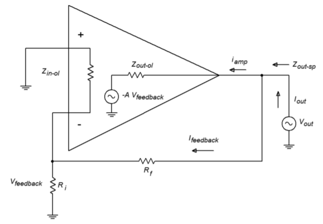
First, notice that 𝐼𝑜𝑢𝑡 is made of two pieces, 𝐼𝑓𝑒𝑒𝑑𝑏𝑎𝑐𝑘 and 𝐼𝑎𝑚𝑝 . If we can find the two impedances associated with these parts, we can simply perform a parallel equivalent in order to determine 𝑍𝑜𝑢𝑡−𝑠𝑝 . The 𝐼𝑓𝑒𝑒𝑑𝑏𝑎𝑐𝑘 portion is very easy to determine. Ignoring the inverting input’s loading effects on 𝑅𝑖 , this impedance is just 𝑅𝑓+𝑅𝑖 . Finding the output impedance of the amplifier itself is a little more involved. 𝐼𝑎𝑚𝑝 is found by taking the drop across 𝑍𝑜𝑢𝑡−𝑜𝑙 and using Ohm’s Law. The voltage across 𝑍𝑜𝑢𝑡−𝑜𝑙 is the difference between 𝑉𝑜𝑢𝑡and the signal created by the feedback path to the inverting input. This signal is −𝐴𝑜𝑙𝑉𝑓𝑒𝑒𝑑𝑏𝑎𝑐𝑘 .
![]()
Since 𝑉𝑓𝑒𝑒𝑑𝑏𝑎𝑐𝑘=𝑉𝑜𝑢𝑡𝛽
![]()
![]()
By using Equation 3.4.8 , this may be simplified to,
![]()
Because
![]()
This is the part of 𝑍𝑜𝑢𝑡−𝑠𝑝 contributed by 𝐼𝑎𝑚𝑝 . To find 𝑍𝑜𝑢𝑡−𝑠𝑝 , just combine the two pieces in parallel:
![]()
With op amps, 𝑅𝑓+𝑅𝑖 is much larger than the first part and can be ignored. For example, a typical device may have 𝑍𝑜𝑢𝑡−𝑜𝑙=75Ω . Even a very modest sacrifice factor will yield a value many times smaller than a typical 𝑅𝑓+𝑅𝑖 combo (generally over 1𝑘Ω ). Discrete circuits using common emitter or common base connections will have larger 𝑍𝑜𝑢𝑡−𝑜𝑙 values, and therefore the feedback path may produce a sizable effect. As in the case of input impedance, 𝑍𝑜𝑢𝑡−𝑠𝑝 is a function of frequency. As 𝑆 decreases as the frequency rises, 𝑍𝑜𝑢𝑡−𝑠𝑝 will increase.
Example 9.4.3
An op amp has the following open-loop specs: 𝑍𝑖𝑛=300𝑘Ω 𝑍𝑜𝑢𝑡=100Ω and A = 50,000. What are the low frequency system input and output impedances if the closed loop gain is set to 100?
First we must find 𝑆
![]()
![]()
![]()
We may now find the approximate solutions.
![]()
![]()
![]()
![]()
The effects are quite dramatic. Note that with such high 𝑍𝑖𝑛 values, op amp circuits may be used in place of FETs in some applications. One example would be the front-end amplifier/buffer in an electrometer (electrostatic voltmeter).
Distortion Effects
As noted earlier, negative feedback lowers static forms of distortion, such as THD. The question, as always, is “How much?” Something like harmonic distortion is internally generated, so we may model it as a voltage source in series with the output source. An example of this model can be seen in Figure 3.4.9 . 𝑉𝑑𝑖𝑠𝑡 is the distortion generator. In the case of a simple input sine wave, 𝑉𝑑𝑖𝑠𝑡 will contain harmonics at various amplitudes (sine waves at integer multiples of the input frequency). These amplitudes are directly related to the input signal’s amplitude. If we assume that 𝑍𝑜𝑢𝑡 is small enough to ignore, 𝑉𝑑𝑖𝑠𝑡 will appear at the output of the open-loop circuit. Thus, the total output voltage is the desired 𝐴𝑉𝑖𝑛plus 𝑉𝑑𝑖𝑠𝑡 .
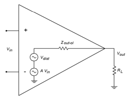
When we add feedback, as in Figure 3.4.10 , this distortion signal is fed back to the inverting input, and because it is now out of phase, it partially cancels the internally generated distortion. Thus the SP distortion signal ( 𝑉𝑑𝑖𝑠−𝑠𝑝 ) is much smaller.

The SP output signal is
![]()
![]()
![]()
We now perform some algebra in order to get this into a nicer form and solve for 𝑉𝑜𝑢𝑡
![]()
![]()
![]()
Remember that 1+𝐴𝑜𝑙𝛽=𝑆 , so,
![]()
![]()
Because 𝐴𝑜𝑙/𝑆 is just 𝐴𝑠𝑝 , this reduces to,
![]()
The internally generated distortion is reduced by the sacrifice factor. As you can see, large sacrifice factors can drastically reduce distortion. An amplifier with 10% THD and a sacrifice factor of 100 produces an effective distortion of only 0.1%. This analysis does assume that the open-loop distortion is not overly grotesque. If the distortion is large, we cannot use this superposition approach (remember, superposition assumes that the circuit is essentially linear). Also, we are ignoring any additional distortion created by feeding this distortion back into the amplifier. For any reasonably linear amplifier, this extra distortion is a second-order effect, and thus constitutes only a small part of the total output signal.
Computer Simulation
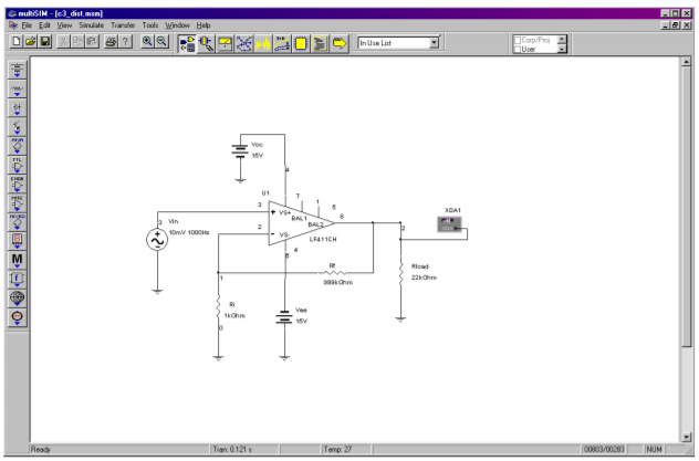
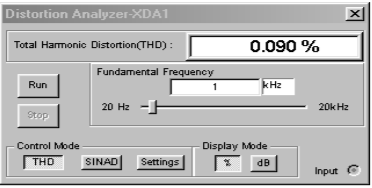
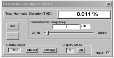
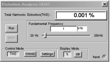
An example of the reduction of distortion is simulated using the Distortion Analyzer from Multisim. A basic amplifier is shown in Figure 3.4.11 . The value for 𝑅𝑓 is changed from 999 k Ω to 99 k Ω to 9 k Ω . 𝑉𝑖𝑛is scaled accordingly so that the output of the amplifier remains at approximately 10 volts. The test frequency was set to 1 kHz and a total of 20 harmonics (up to 20 kHz) were used in the analysis. Using the LF411 op amp, the high gain version shows a THD of 0.09%. Reducing the gain by a factor of 10 (and thus increasing sacrifice factor by 10 fold) yields a THD of 0.011%. Finally, a further 10 fold reduction of gain yields a THD of 0.001%. Although the reduction in distortion is not exactly a factor of 10 each time, the trend can be seen clearly. The precise distortion values will depend on the accuracy of the op amp model used, the test frequency, and the number of harmonics kept in the analysis. 20 kHz was chosen here because that represents the upper limit of human hearing, and thus it would be appropriate for an audio amplifier.
As we have seen, the sacrifice factor is a very useful item. Our gain, distortion, and 𝑍𝑜𝑢𝑡 are all reduced by 𝑆 , while 𝑓2 and 𝑍𝑖𝑛 are increased by 𝑆 .
Noise
It is possible to model noise effects in much the same way as we just modeled distortion effects. By doing so, you will discover that noise can also be decreased by a large amount. Unfortunately, there is one major flaw. Unlike our distortion generator, a noise generator will produce a signal that is not dependent on the input signal. The net result is that although the noise level does drop by the sacrifice factor, so does the desired output signal. Thus, the signal-to-noise ratio at the output is unchanged. In contrast, the distortion signal is proportional to the input signal, so that when the desired signal is cut by 𝑆 , the distortion signal sees a further cut by 𝑆 (i.e., the distortion drops by 𝑆 relative to the desired signal). As a matter of fact, it is quite possible that the noise produced in following stages may add up to more noise than the circuit had without feedback. Sad but true, negative feedback doesn’t help us when it comes to signal-to-noise ratio.
Parallel-Series (PS)
The Parallel-Series connection is the opposite of the Series-Parallel form. PS negative feedback is used to make the ideal current amplifier. Its gain is dimensionless, but for convenience, it is normally given the units A/A (amps per amp). It produces a low 𝑍𝑖𝑛 (perfect for sensing 𝐼𝑖𝑛 ) and a high 𝑍𝑜𝑢𝑡 (making for an ideal current source). An example of PS is shown in Figure 3.4.12 .
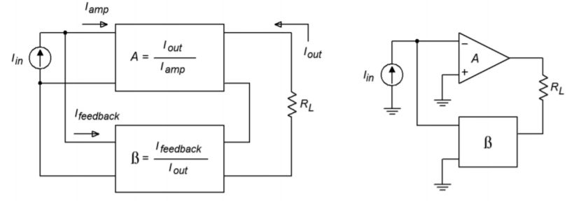
The signal source’s current splits in two, with part going into the amplifier, and part going through the feedback network. This is how you know that you have a parallel input connection. The output current on the other hand, passes through the load and then enters the feedback network, indicating a series output connection. Note that this general model is an inverting type, and that the load is floating (i.e., not ground referenced). It is possible though to use ground referenced loads with some additional circuitry. As PS is used for current amplification, let’s see how we can find the current gain. Figure 3.4.13 will help us along. PS current gain is defined as:
![]()
(9.4.11)
The signal source’s current splits into two paths, so
![]()
(9.4.12)
Because 𝐼𝑎𝑚𝑝 times the amplifier’s open-loop current gain is 𝐼𝑜𝑢𝑡 , we can also say,
![]()
9.4.13)
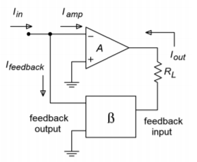
The feedback network is nothing more than a current divider, where the feedback network’s output ( 𝐼𝑓𝑒𝑒𝑑𝑏𝑎𝑐𝑘 ) is 𝛽 times smaller than its input ( 𝐼𝑜𝑢𝑡 ). Don’t let the arbitrary current direction fool you – the feedback “flow” is still from right to left, as always. In this case the amplifier is sinking current instead of sourcing it. As 𝛽 is just a fraction, we may say
![]()
![]()
![]()
(9.4.14)
By substituting Equation 3.4.14 into Equation 3.4.12 we see that
![]()
![]()
(9.4.15)
After substituting this into Equation 3.4.11 we find that
![]()
or, with the help of Equation 3.4.13
![]()
(9.4.16)
To make a long story short, the open-loop gain is reduced by the sacrifice factor. (Where have we seen this before?) The one item that you should note is that we have used only current gains in our derivation (compared to voltage gains in the SP case).
It is possible to perform a derivation using the open-loop voltage gain; however, the results are basically the same, as you might have guessed. Once again, our approximation for gain can be expressed as 1/𝛽 .
Example 3.4.4
A co-worker asks you to measure the output current of a circuit that she’s just built. If all is working correctly, this circuit should produce 100 microamps. Unfortunately, your hand-held DMM will only accurately measure down to 1 milliamp. It is 10 times less sensitive than it needs to be. In order to be read accurately, the current will need to be boosted. Does the amplifier of Figure 3.4.14 have the current gain you need?
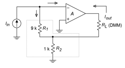
If we are using an op amp, we can assume that 𝐴𝑝𝑠=1/𝛽 . The question then becomes, “what is 𝛽 ?” 𝛽 is the current divider ratio. The resistors 𝑅1 and 𝑅2 make up the current divider. The output current splits between 𝑅1 and 𝑅2 , where the 𝑅1 path is 𝐼𝑓𝑒𝑒𝑑𝑏𝑎𝑐𝑘 . According to the current divider rule,
![]()
Consequently the gain magnitude is
![]()
![]()
This Equation looks a lot like the one in the SP example! Solving for 𝐴𝑝𝑠 yields
![]()
![]()
Yes, this circuit has just the gain you need. All you have to do is connect your co-worker’s circuit to the input, and replace the load resistor with your hand-held DMM. Note that most DMMs are floating instruments and are not tied to ground (unlike an oscilloscope), so using it as a floating load presents no problems. The accuracy of the gain (and thus your measurement) depends on the accuracy of the resistors and the relative size of the op amp’s input bias current. Therefore, it would be advisable to use a bi-FET type device (i.e., an op amp with an FET diff amp) and precision resistors.
PS Impedance Effects
As you have seen, the gain derivation for PS is similar to that for SP. The same is true for the impedance equations. First, we’ll take a look at input impedance with Figure 3.4.15 .
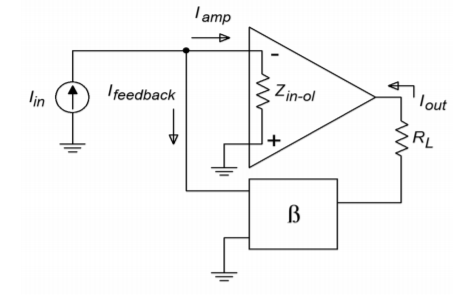
As always, we start with our base definition,
![]()
Recalling Equation 3.4.15 , this can be rewritten as,
![]()
(9.4.17)
𝑉𝑖𝑛is merely the voltage that appears from the inverting input to ground. By using Ohm’s Law, we can say,
![]()
Where 𝑍𝑖𝑛−𝑜𝑙 is the open-loop input impedance. Finally, substituting this into Equation 3.4.17 gives,
![]()
![]()
The input impedance is lowered by the sacrifice factor. If you’re starting to wonder whether everything is altered by the sacrifice factor, the answer is, yes. This is, of course, an approximation. What do you think is going to happen to the output impedance? At this point, it shouldn’t be too surprising. For this proof, refer to Figure 3.4.16 . We shall use the same general technique to find 𝑍𝑜𝑢𝑡 as we did with the SP configuration. In this case we replace the load with a current source, and then determine the resulting output voltage.
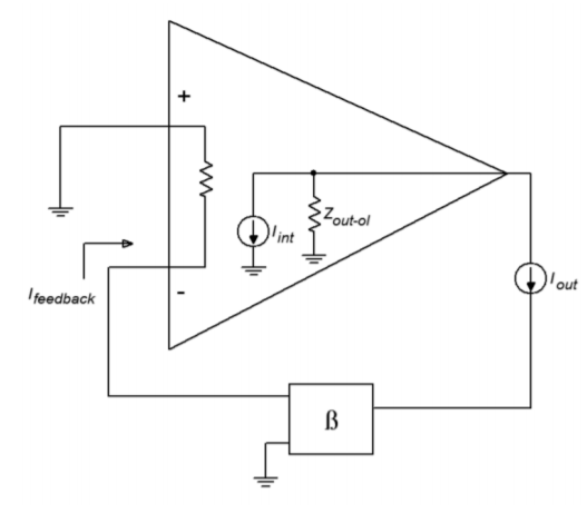
Note that the input signal current source is opened. The output current drives the feedback network and produces the feedback current. The feedback current is then multiplied by the amplifier’s open-loop current gain. Because the feedback current enters the inverting input, the internal source is sinking current. Because we are driving the circuit from the output,
![]()
𝑉𝑜𝑢𝑡is found through Ohm’s Law
![]()
We now expand on our currents.
![]()
![]()
![]()
![]()
![]()
Finally, we see that,
![]()
![]()
As expected, the series output connection increased 𝑍𝑜𝑢𝑡 by the sacrifice factor. The remainder of the PS equations are essentially those used in our earlier SP work. Once again, the bandwidth will be increased by 𝑆 , and the distortion will be reduced by 𝑆 . This is also true for the Parallel-Parallel and Series-Series connections. As a matter of fact, the 𝑍𝑖𝑛 and 𝑍𝑜𝑢𝑡 relations are just what you might expect. The proofs are basically the same as those already presented, so we won’t go into them. Suffice to say that parallel connections reduce the impedance by 𝑆 , and series connections increase it by 𝑆 .
Parallel-Parallel (PP) and Series-Series (SS)
Unlike our two earlier examples, the concept and modeling of gain is not quite as straight forward in the Parallel-Parallel and Series-Series cases. These forms do not produce gain, so to speak. They are neither voltage amplifiers, nor current amplifiers. Instead, these connections are used as transducers. Parallel-Parallel turns an input current into an output voltage. It is shown in Figure 3.4.17 .

Series-Series turns an input voltage into an output current. It is shown in Figure 3.4.18 . Our normal gain and feedback factors now have units associated with them. Because our output versus input quantities are measured in volts-per-amp (PP) or amps-per-volt (SS), the appropriate units for our factors are Ohms and Siemens. To be specific, we refer to our PP gain as a transresistance value, and the SS gain as a transconductance value. Although it is quite possible (and useful) to derive formulas for gain based on these, it is often done only for discrete designs. Quite simply, you cannot find transresitance or transconductance values on typical op amp data sheets.
Fortunately, we can make a few approximations and create some very useful circuits utilizing PP and SS feedback with op amps. These design and analysis shortcuts are presented in the next chapter, along with practical applications.


