12.4 Switching Regulators
The major cause of the inefficiency of a linear regulator is that its pass transistor operates in the linear region. This means that it constantly sees both a high current and a high (or at least moderate) voltage. The result is a sizable power dissipation. In contrast, switching regulators rely on the efficiency of the transistor switch. When the transistor is off, no current flows, and thus, no power is dissipated. When the transistor is on (in saturation), a high current flows, but the voltage across the transistor ( 𝑉𝑐𝑒(𝑠𝑎𝑡) ) is very small. This results in modest power dissipation. The only time that both the current and voltage are relatively large at the same time is during the switching interval. This time period is relatively short compared to cycle time, so again, the power dissipation is rather small.
Switching the pass transistor on and off can be very efficient, but unfortunately, the resulting pulses of current are not appropriate for most loads. Some way of smoothing out the pulses into a constant DC level is needed. One way to do this is through an inductor/capacitor arrangement. This concept is essential to the switching regulator.
Although the switching regulator does offer an increased efficiency over the linear regulator, it is not without its detractions. First of all, switching regulators tend to be more complex than linear types. This complexity may outstrip the efficiency advantage, particularly for low-power designs. Some of the newer “single chip” switching regulators make switching power supply design almost as straightforward as linear design, so this problem is not quite as great as it once was. The other major problem is that the switching process can create a great deal of radiated electrical noise. Without proper shielding and similar precautions, the induced noise signals can produce grave interference in nearby analog or digital circuits. In spite of these obstacles, switching power supplies have seen great acceptance in a variety of areas, including powering personal computers.

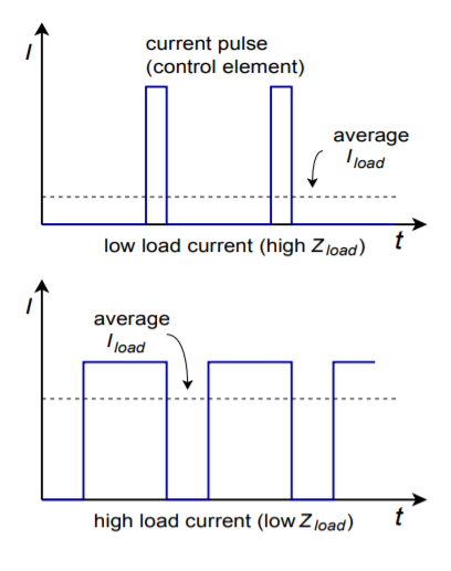
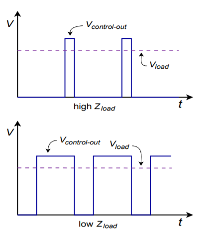
A basic switching regulator outline is shown in Figure 8.4.1 . Once again, a control device is used to adjust the incoming signal. Unlike the linear regulator, the signal out of the control element is a pulse train. In order to produce a smooth DC output, the pulse train is passed through a capacitor/inductor network. The heart of the circuit is the pulse-width modulator. This circuit creates a variable duty cycle pulse waveform, which alternately turns the control element on and off. The duty cycle of the pulse is proportional to the load current demand. Low load impedances require large currents and, thus, will create pulse trains with long “on” times. The peak value of the pulses will tend to be much greater than the average load current demand, however, if this current pulse is averaged over one cycle, the result will equal the load current demand. Effectively, the 𝐿𝐶 network serves to integrate the current pulses. This is shown graphically in Figure 8.4.2 . Because the lower load impedance is receiving a proportionally larger current, the load voltage remains constant. This is shown graphically in Figure 8.4.3 .
Due to the constant charging and discharging of the 𝐿 and 𝐶 components, switching regulators tend to respond to load changes somewhat slower than linear regulators do. Also, if the frequency of the switching pulse is high, the required sizes for 𝐿 and 𝐶 may be reduced, resulting in a smaller circuit and possible cost reductions. Many switching regulators run in the 20 kHz to 100 kHz region. The practical upper limit for switching speed is determined by the speed of the control element. Devices with fast switching times will prove to be more efficient. Power FETs are very attractive for this application because of their inherent speed and low drive requirements. Their negative temperature coefficient of transconductance also helps reduce thermal runaway problems. For the highest powers, bipolar devices are often the only choice. Finally, it is possible to configure many switchers for step down, step up, or inverter operation. As an example, we will investigate the step down, or buck, configuration.
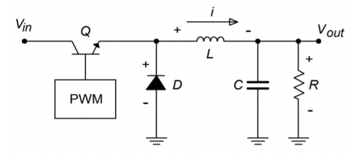
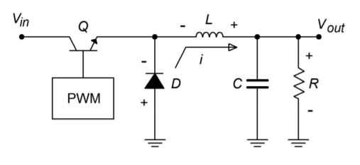
A block diagram of a step down switching regulator is shown in Figure 8.4.4 . Here is how it works: When the transistor, 𝑄 , is on, current flows through 𝑄 , 𝐿 , and the load. The inductor current rises at a rate equal to the inductor voltage divided by the inductance. The inductor voltage is equal to the input voltage minus the load voltage and the transistor’s saturation potential. While 𝐿 is charging (i.e., 𝐼𝐿<𝐼𝑙𝑜𝑎𝑑 ), 𝐶 provides load current. When 𝑄 turns off, the inductor’s magnetic field starts to collapse causing an effective polarity reversal. In other words, the inductor is now acting as a source for load current. At this point, diode 𝐷 is forward biased, effectively removing the left portion of the circuit. 𝐿 also supplies current to capacitor 𝐶 during this time period. Eventually, the inductor current will drop below the value required by the load, and 𝐶 will start to discharge, making up the difference. Before 𝐿 completely discharges, the transistor switch will turn back on, repeating the cycle. Because the inductor is never fully discharged, this is called continuous operation. Discontinuous operation is also possible, although we will not pursue it here. One point worth noting is that for proper continuation of this cycle, some load current draw must always be present. This minimum level can be achieved through the use of a bleed resistor in parallel with the load.
The values for 𝐶 and 𝐿 are dependent on the input and output voltages, desired output current, the switching frequency, and the particulars of the switching circuit used. Manufacturers generally give look-up tables and charts for appropriate values and/or formulas. Earlier switching ICs contained the necessary base components and required only a moderate amount of external circuitry. The newest ICs may be configured with no more than three or four external passive parts.
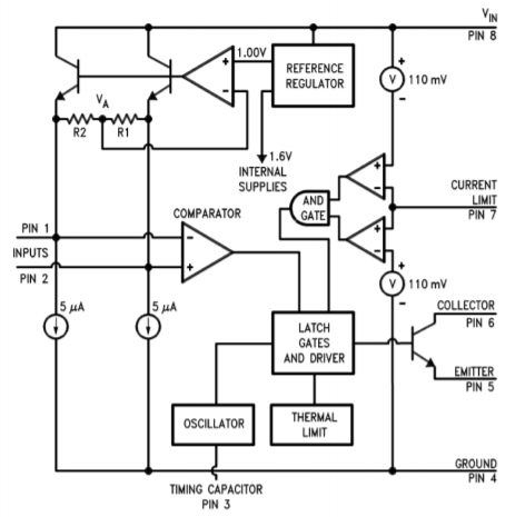
One example of a switch mode regulator is the LM3578A. A functional diagram of the inner workings of this IC is shown in Figure 8.4.5 . The AND gates, comparator, oscillator, and associated latches combine to form the pulse-width modulator. Notice that this circuit includes an internal reference and mediumpower switching transistor. Thermal shutdown and current limiting are available. The circuit will operate at inputs up to 40 V and can produce output currents up to 750 mA. The maximum switching frequency is 100 kHz. Step up, step down, and inverter configurations are all possible with this device. To make the design sequence is fast as possible, the manufacturer has included a design chart. This is shown in Figure 8.4.6 . As with virtually all highly specialized ICs, specific design equations only apply to particular devices, and probably cannot be used with ICs that produce similar functions. Consequently, it is recommended that you do not memorize these formulas!

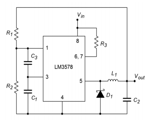
A step down regulator using the LM3578A is shown in Figure 8.4.7 . 𝐶1 is the frequency-selection capacitor and can be found from the manufacturer’s chart. 𝐶3 is necessary for continuous operation and is generally in the vicinity of 10 to 30 pF. 𝐷1 should be a Schottky-type rectifier. 𝑅1 and 𝑅2 set the step down ratio (they are functionally the same as 𝑅𝑓 and 𝑅𝑖 in the previous work). 𝑅3 sets the current limit. Finally, 𝐿1 and 𝐶2 are used for the final output filtering.
The relevant equations from the manufacturer’s data sheets are:
![]()
![]()
![]()
![]()
![]()
Where 𝐼𝑠𝑤(𝑚𝑎𝑥) is the maximum current through the switching element, and 𝑉𝑟𝑖𝑝𝑝𝑙𝑒 is in peak-to-peak volts. Some values may be found using the look-up chart method shown in Figure 8.4.6 .
Example 8.4.1
Using the LM3578A, design a step down regulator that delivers 12 V from a 20 V source, with 200 mA of load current. Use an oscillator frequency of 50 kHz, and a discontinuity factor of 0.2 (20%). Ripple should be no more than 40 mV.
First determine the 𝑅1 and 𝑅2 values. 𝑅2 is arbitrarily chosen at 10 k Ω .
![]()
![]()
![]()
![]()
![]()
![]()
![]()
Note that 𝑅3 will always be 0.15 Ω for this circuit form
From the oscillator graph, 𝐶1 is estimated at 1700 pF, and 𝐶3 is set to 20 pF, as suggested by the manufacturer.
![]()
![]()
![]()
![]()
![]()
![]()
![]()
![]()
![]()
To be on the conservative side, 𝐶2 is usually set a bit higher, so a standard 33 𝜇 F or 47 𝜇 F might be used.
A basic inverting switcher is shown in Figure 8.4.8 . This circuit produces a negative output potential from a positive input. It works as follows: When the transistor switch is closed, the inductor L is charged. Diode 𝐷 is in reverse bias, as its anode is negative. When the switch opens, the inductor’s collapsing field causes it to appear as a source of opposite polarity. The diode is forward-biased because its cathode is now forced to be lower than its anode. The inductor is now free to deliver current to the load. Eventually, the inductor will discharge to the point where the transistor switch will turn back on. While the inductor is charging, capacitor 𝐶 will supply the load current. The process repeats, thus maintaining a constant output potential.

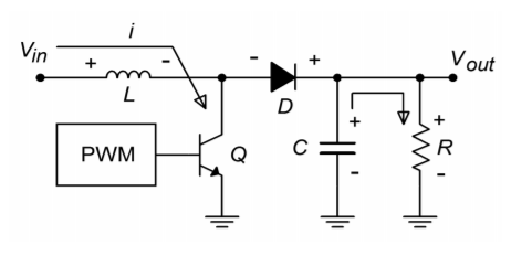
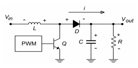
A basic step up switcher is shown in Figure 8.4.9 . This variation is used when a potential greater than the input is desired, such as deriving a 15 V supply from an existing 5 V source. Here is how the circuit works: When the transistor switch is closed, the inductor 𝐿 charges. During this time period, the capacitor 𝐶 is supplying load current. Because the output potential will be much higher than the saturation voltage of the transistor switch, the diode 𝐷 will be in reverse bias. When the transistor turns off, the magnetic field of the inductor collapses, causing the inductor to appear as a source. This potential is added to the driving source potential, as these two elements are in series. This combined voltage is what the load sees; hence, the load voltage is greater than the driving source. Eventually, the inductor will discharge to the point where the transistor switches back on, thus reverse-biasing the diode and recharging 𝐿 . The capacitor will continue to supply load current during this time. This process will continue in this fashion, producing the desired output voltage.
For the step up and inverter forms, other sets of equations are used for the LM3578A. Although the design sequence is certainly not quite as straightforward as in the linear regulator circuits, it is definitely not a major undertaking, either. If 750 mA is not sufficient, an external pass transistor may be added to the LM3578A. Other switching regulator ICs are available from different manufacturers. Each unit operates on the same basic principle, but the realization of the design may take considerably different routes. Specific device data sheets must be consulted for each model.
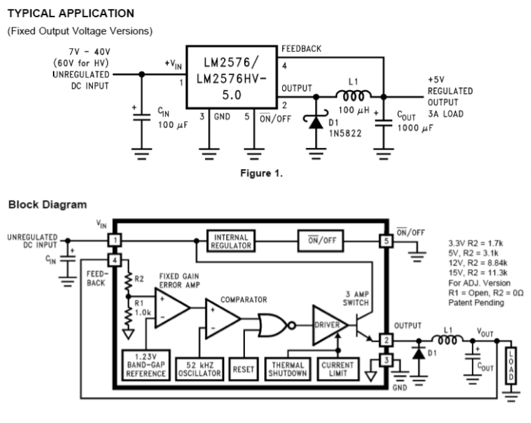
For specific applications, some manufacturers offer switching regulators that are almost drop-in replacements for basic 3-pin linear regulators. These devices are not nearly as flexible as the generic switching regulator ICs, though. A good example is the LM2576 regulator. This is a 3 A output, step down regulator (i.e., buck-mode only). It is available at a variety of output potentials ranging from 3.3 V to 15 V. An adjustable version is also available. A block diagram and typical circuit are shown in Figure 8.4.10 . As you can see, a typical fixed output design requires a minimum of external components: 2 capacitors, an inductor, and a diode. Other members of this family include the LM2574 0.5 A step down regulator, and the LM2577 step up regulator.
