
10.6 Problems
Review Questions
- What forms of feedback are used for the inverting and noninverting voltage amplifiers?
- What forms of feedback are used for the current-to-voltage and voltage-to-current transducers?
- What form of feedback is used for the inverting current amplifier?
- What are the op amp analysis idealizations?
- What is virtual ground?
- What is a summing amplifier?
- How can output current by increased?
- What circuit changes are needed in order to bias an op amp with a unipolar supply?
- What operational parameters change when a circuit is set up for single supply biasing?
- How might a circuit’s gain be controlled externally?
- What is meant by the term “floating load”?
Problems
Analysis Problems
- What is the voltage gain in Figure 4.6.1 ? What is the input impedance?
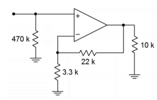
Figure 4.6.1 - What is the voltage gain for the first stage of Figure 4.6.2 ? What is the input impedance?

Figure 4.6.2 - What is the voltage gain for the second stage of Figure 4.6.2 ? What is the input impedance?
- What is the system voltage gain in Figure 4.6.24.6.2? What is the input impedance?
- If the input to Figure 4.6.2 is -52 dBV, what is 𝑉′𝑜𝑢𝑡 ?
- What is the voltage gain in Figure 4.6.3? What is the input impedance?
- If the input voltage to the circuit of Figure 4.6.3 is 100 mV, what is 𝑉𝑜𝑢𝑡?
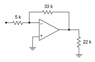
Figure 4.6.3 - What is the system input impedance in Figure 4.6.4 ? What is the system gain?

Figure 4.6.4 - Redesign Figure 4.6.4 for an input impedance of 20 k Ω .
- Given an input current of 2 𝜇 A, what is the output voltage in Figure 4.6.5 ?
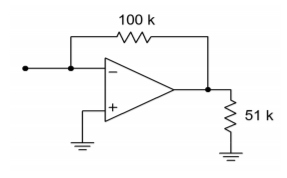
Figure 4.6.5 - What is the meter deflection in Figure 4.6.6 if the input voltage is 1 V?
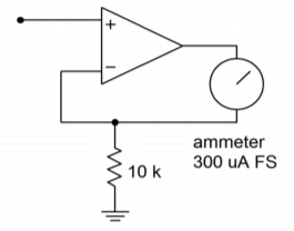
Figure 4.6.6 - What input voltage will produce full-scale deflection in figure 4.6.6 ?
- Determine a new value for the 10 k Ω resistor in Figure 4.6.6 such that a 0.1 V input will produce full-scale deflection.
- What is the current gain in Figure 4.6.7 ?
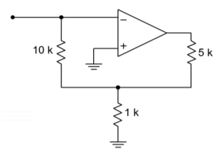
Figure 4.6.7 - What is the maximum input current in Figure 4.6.7 , assuming the circuit is running off of ± 15 V supplies, and the op amp has a maximum output current of 25 mA?
- If the differential input signal is 300 mV in Figure 4.6.8 , what is 𝑉𝑜𝑢𝑡?
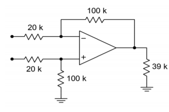
Figure 4.6.8 - Determine new values for the voltage divider resistors in Figure 4.6.8 , such that the resulting input impedance is balanced.
Design Problems
- Design a noninverting amplifier with a voltage gain of 32 dB and an input impedance of 200 k Ω.
- Design a voltage follower with a gain of 0 dB.
- Design an inverting amplifier with a voltage gain of 14 dB and an input impedance of 15 k Ω.
- Design a current-to-voltage transducer such that a 20 𝜇 A input current will produce a -1 V output.
- Design a voltage-to-current transducer such that a 100 mV input will produce a 1 mA output.
- Design a current amplifier with a gain of -20.
- Design a differential amplifier with a gain of 18 dB and a balanced input impedance of 25 k Ω per input.
- Design a voltage to current transducer with a transconductance of 1 mS. If 𝑉𝑖𝑛is 200 mV, what is 𝐼𝑜𝑢𝑡 ?
- Design a current to voltage transducer with a transresistance of 10 k Ω . If the input current is 500 𝜇 A, what is 𝑉𝑜𝑢𝑡?
- Redesign the circuit of Figure 4.6.1 for single supply operation (don’t bother calculating capacitor values).
- Redesign the circuit of Figure 4.6.3 for single supply operation (don’t bother calculating capacitor values).
- Design a summing amplifier such that channel 1 has a gain of 10, channel 2 has a gain of 15, and channel 3 has a gain of 5. The minimum channel input impedance should be 1 k Ω .
- Determine capacitor values for Problem 27 if the lower break frequency 𝑓1 , is set to 20 Hz.
- Determine capacitor values for Problem 28 if the lower break frequency f1, is set to 10 Hz.
Challenge Problems
- Design a three channel summing amplifier such that: channel 1 𝑍𝑖𝑛≥10𝑘Ω , 𝐴𝑣 = 6 dB; channel 2 𝑍𝑖𝑛≥22𝑘Ω , 𝐴𝑣 = 10 dB; and channel 3 𝑍𝑖𝑛≥5𝑘Ω , 𝐴𝑣 = 16 dB
- Assuming 10% resistor values, determine the production gain range for Figure 4.6.1 .
- Assuming 5% resistor values, determine the highest gain produced in Figure 4.6.2 .
- Design an inverting amplification circuit with a gain of at least 40 dB, and an input impedance of at least 100 k Ω . No resistor used may be greater than 500 k Ω . Multiple stages are allowed.
- Redesign the circuit of Figure 4.6.3 as a voltmeter with 500 mV, 2 V, 5 V, 20 V, and 50 V ranges.
- Assuming 1% precision resistors and a meter accuracy of 5%, what range of input values may produce a full-scale reading of 2 V, for the circuit of Problem 36?
- Design an amplifier with a gain range from -10 dB to +20 dB, with an input impedance of at least 10 k Ω .
- Design an amplifier with a gain range from 0 to 20. The input impedance should be at least 5 k Ω .
- What is the input impedance in Figure 4.6.9 ? What is 𝐴𝑣 ?
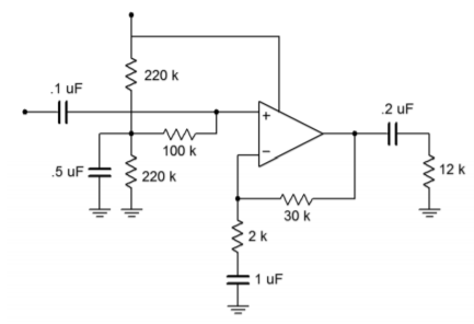
Figure 4.6.9 - How much power supply ripple attenuation does the input biasing network of Figure 4.6.9 produce (assume 𝑓𝑟𝑖𝑝𝑝𝑙𝑒 = 120 Hz)?
- Assume that the circuit of Figure 4.6.10 utilizes a standard 20 mA output op amp. If the output devices are rated for a maximum collector current of 5 amps and a Beta of 50, what is the maximum load current obtainable?
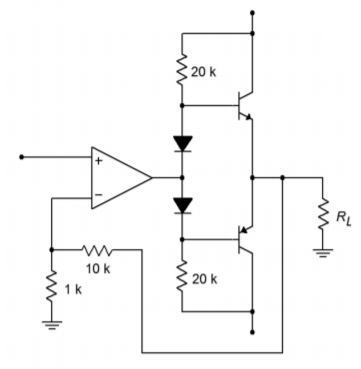
Figure 4.6.10 - What are the voltage gain and input impedance in Figure 4.6.10 ?
- Given a summer based on Figure 4.2.22, sketch the output waveform if 𝑅1=𝑅2= 10 k Ω , 𝑅3=𝑅𝑓= 30 k Ω , 𝑅𝑖 = 15 k Ω , 𝑉1 = 0.3 V DC, 𝑉2=0.1sin2𝜋50𝑡 and 𝑉3=−0.2sin2𝜋200𝑡 .
- Prove Equation 4.2.15 for the case when all resistors are of equal value.
Computer Simulation Problems
- Simulate the operation of the circuit in Figure 4.2.9. Verify the output voltage and the virtual ground at the inverting input.
- Use a simulator to verify the maximum and minimum gains of the circuit in Figure 4.2.11.
- Use a simulator to verify the load current and the voltage of the circuit in Figure 4.2.17.
- Verify the output potential of the circuit in Figure 4.2.20.
- Simulate the output voltage of the circuit of Figure 4.6.4 for the following inputs:
- 𝑉𝑖𝑛=0.1 VDC,
- 𝑉𝑖𝑛(𝑡)=1sin2𝜋10𝑡,
- 𝑉𝑖𝑛=5 VDC.
Also, note the potential at the output of the first stage. How might your op amp model affect the results?
- Simulate the circuit in Figure 4.2.27. Determine the output potential for the following inputs:
-
- 𝑉𝑖𝑛+(𝑡)=0.1sin2𝜋10𝑡 , 𝑉𝑖𝑛−(𝑡)=0.1sin2𝜋10𝑡,
- 𝑉𝑖𝑛+(𝑡)=0.1sin2𝜋10𝑡 , 𝑉𝑖𝑛−(𝑡)=−0.1sin2𝜋10𝑡.
-
- Simulate the circuit of Figure 4.6.10 , and determine the output of the circuit and op amp for inputs of 0.1 V DC and 1 V DC.
Use the space below creatively. Draw a cartoon. Compose a song. Write a limerick. Whatever works for you. If you’re stuck, try starting with this: ♫
