11.3 Gain-Bandwidth Product
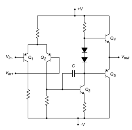
The open loop frequency response of a general-purpose op amp is shown in Figure 5.3.1𝑎 . Although the exact frequency and gain values will differ from model to model, all devices will exhibit this same general shape and 20 dB per decade rolloff slope. This is because the lag break frequency (𝑓𝑐) is determined by a single capacitor called the compensation capacitor. This capacitor is usually in the Miller position (i.e., straddling input and output) of an intermediate stage, such as 𝐶 in Figure 5.3.1𝑏 . Although this capacitor is rather small, the Miller effect drastically increases its apparent value. The resulting critical frequency is very low, often in the range of 10 to 100 Hz. The other circuit lag networks caused by stray or load capacitances are much higher, usually over 1 MHz. As a result, a constant 20 dB per decade rolloff is maintained from 𝑓𝑐 up to very high frequencies. The remaining lag networks will not affect the open-loop response until the gain has already dropped below zero dB.
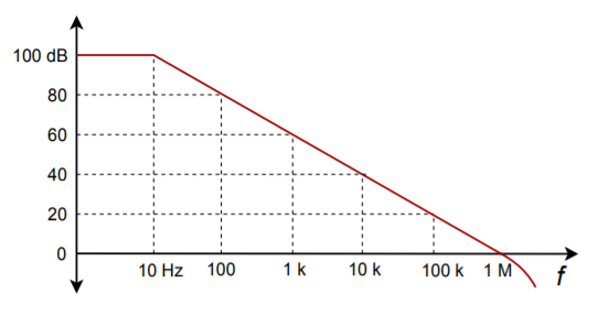
This type of frequency response curve has two benefits: (1) The most important benefit is that it allows you to set almost any gain you desire with stability. Only a single network is active, thus satisfactory gain and phase margins will be maintained. Therefore, your negative feedback never turns into positive feedback (as noted in Chapter Three). 2) The product of any break frequency and its corresponding gain is a constant. In other words, the gain decreases at the same rate at which the frequency increases. In Figure 5.3.1 , the product is 1 MHz. As you might have guessed, this parameter is the gain-bandwidth product of the op amp (GBW). GBW is also referred to as 𝑓𝑢𝑛𝑖𝑡𝑦 (the frequency at which the open loop gain equals one). You will find both terms used on manufacturer’s spec sheets.
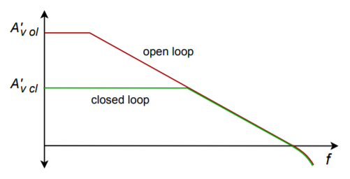
As you already know, operating an op amp with negative feedback lowers the midband gain. To a first approximation, this gain will continue until it reaches the open loop response. At this point, the closed loop response will follow the open-loop rolloff. Remember, this is due to the reduction in loop gain, as seen in Chapter Three. This effect is shown in Figure 5.3.2 .
By knowing GBW and the gain, the associated break frequency can be quickly determined. For the inverting and noninverting voltage amplifiers,
![]()
(5.3.1)
The use of noise gain versus ordinary voltage gain simplifies things and actually makes the results a bit more accurate. Noise gain is the same for both the inverting and noninverting voltage amplifiers. The use of noise gain helps us to take into account the true (non-ideal) feedback effects and circuit imperfections. An example of these limitations is that the open loop gain of an op amp is never infinite. To find the noise gain for any circuit, short all voltage sources and open all current sources. The only item remaining for each source should be its internal resistance. At this point, simplify the circuit as required, and find the gain from the noninverting input to the output of the op amp. This gain is the noise gain. For the standard inverting and noninverting voltage amplifiers, we find
![]()
Noise gain is the same as ordinary voltage gain for the noninverting voltage amplifier, but is one unit larger than the inverting amplifier’s ordinary gain (𝑅𝑓/𝑅𝑖) . The deviation is only noticeable at lower gains. This does imply though, that for the same gain, noninverting amplifiers will exhibit a higher break frequency than inverting types. Thus, for maximum bandwidth with low gain circuits, the noninverting form is generally preferred. The worst case occurs with an ordinary voltage gain of 1. For the noninverting configuration, the noise gain will also equal 1, and the closed loop bandwidth will equal 𝑓𝑢𝑛𝑖𝑡𝑦 . On the other hand, an inverting amplifier with a voltage gain of 1 will produce a noise gain of 2 and will exhibit a small-signal bandwidth of 𝑓𝑢𝑛𝑖𝑡𝑦/2 . Never use the gain in dB form for this calculation!
Example 5.3.1
Using a 741 op amp, what is the upper break frequency for a noninverting amplifier with a gain of 20 dB?
A 741 data sheet shows a typical GBW of 1 MHz. The noise gain for a noninverting amplifier is the same as its ordinary gain. Converting 20 dB into ordinary form yields a gain of 10.
![]()
![]()
![]()
So, the gain is constant at 10 up to 100 kHz. Above this frequency the gain rolls off at 20 dB per decade.
Example 5.3.2
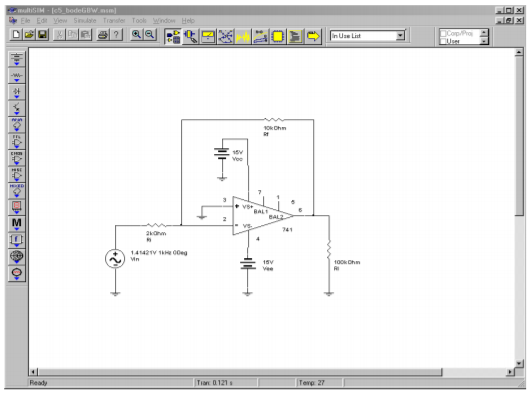
Sketch the frequency response of the circuit in Figure 5.3.3

This is an inverting voltage amplifier. The gain is
![]()
![]()
![]()
For noise gain
![]()
![]()
![]()
From a data sheet, GBW for a 741 is found to be 1 MHz.
![]()
![]()
![]()

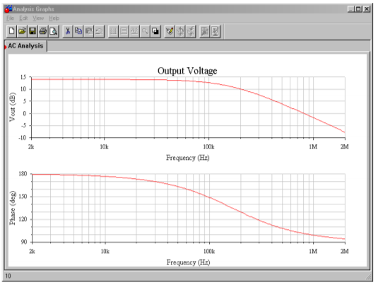
The resulting gain Bode plot is shown in Figure 5.3.4 . Note that if a “faster” op amp is used (i.e., one with a higher GBW, such as the LF411), the response will extend further. As you might guess, faster op amps are more expensive.
Computer Simulation
The simulation results for Example 5.3.2 are also shown in Figure 5.3.4 . The low frequency gain agrees with the hand calculation of approximately 14 dB. The 3 dB down point (𝑓2) also agrees with the calculated break of approximately 167 kHz.
It is important to note that the simple dependent source model presented in Chapter Two cannot be used because it does not have the proper frequency response. Instead, manufacturers offer accurate models for their op amps. There are several variations on the theme. The model presented here is typical. It is fairly complex and is quite accurate. The op amp model is comprised of two basic parts, a differential amplifier input portion and a dependent source output section. The input portion utilizes a pair of NPN transistors with simple resistors for the loads ( 𝑅𝐶1 and 𝑅𝐶2 ). Resistors 𝑅𝐸1 and 𝑅𝐸2 serve as swamping or emitter-degeneration resistors. The tail-current source is set by the independent source 𝐼𝐸𝐸 . The non-ideal internal impedance and frequency limitations of this current source are taken into account by 𝑅𝐸 and 𝐶𝐸 , whereas 𝐶1 helps to model the high frequency loading of the diff amp’s output. The output portion revolves around a series of voltage-controlled current sources. GCM models common mode gain, GA models the ordinary gain, and 𝑅2 serves as the combined internal impedance of these sources. 𝐶2 is the system compensation capacitor and has a value of 30 pF. 𝑅𝑂1 and 𝑅𝑂2 serve to model the output impedance of the op amp. Diodes 𝐷1 through 𝐷4 and voltage sources 𝐸𝐶 , 𝑉𝐶 , and 𝑉𝐸 model the limits of the op amp’s class AB output stage.

In spite of their accuracy, models such as this are time consuming and tedious to recreate. Fortunately, many manufacturers offer simulation models for their components in library form. To use these models, all you need to do is reference the appropriate part number from the library. The op amp models normally use typical rather than worst-case values.
Example 5.3.3
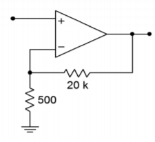
Determine the minimum acceptable 𝑓𝑢𝑛𝑖𝑡𝑦 for the circuit of Figure 5.3.5 if response should extend to at least 50 kHz.
![]()
![]()
![]()
![]()
![]()
![]()
For this application, a stock 741 would not be fast enough; however, a 411 would be fine. From the foregoing, it is apparent that there is a direct trade off between circuit gain and high frequency performance for a given device. For an application requiring both high gain and wide bandwidth, a multistage approach should be considered.
Multi-stage Considerations
By combining two or more wide-bandwidth, low-gain stages, a single high-gain, wide-bandwidth system may be produced. Although the overall system gain will simply be the combination of the individual stage gains, the upper break frequency calculation can be a little tricky. Chances are, in a multi-stage op amp design all stages will not exhibit the same upper break frequency. In this case the system’s upper break is approximately equal to the lowest of the stage 𝑓𝑐𝑠 . In other words, the system is treated as though it was a discrete stage with multiple lag networks. On the other hand, if the break frequencies are close, this approximation can lead to a sizable error. This is best illustrated with a quick example. Imagine two stages exhibiting a 100 kHz break. If each stage produces a 3 dB loss at 100 kHz, it is obvious that the cascaded system must be producing a 6 dB loss at 100 kHz. Therefore, the system’s critical frequency (i.e., -3 dB point) must be somewhat lower than 100 kHz (to be exact, it is the frequency at which each stage produces a 1.5 dB loss). Taking this a step further, if we cascade three identical stages, the total loss at 100 kHz will be 9 dB. The system break will be the point at which each of the three stages produces a 1 dB loss. The more identical stages that are added, the lower the effective break becomes. If we make a few assumptions about the exact shape of the rolloff curve, we can reduce this to a simple equation. In Chapter One, we derived the general Equation describing the amplitude response of a lead network (1.3.3). In a similar vein, the response for a lag network may be determined to be
![Rendered by QuickLaTeX.com \[A_v = \frac{1}{\sqrt{1+ \frac{f^2}{f_c^2}}} \]](https://pressbooks.nscc.ca/app/uploads/quicklatex/quicklatex.com-ded079bb0e5c2b5efd24efaad1b6f4d0_l3.png)
(5.3.2)
Where f is the frequency of interest and 𝑓𝑐 is the critical frequency.
It is more convenient to write this Equation in terms of a normalized frequency of interest. Instead of being expressed in Hertz, the frequency of interest is represented as a factor relative to 𝑓𝑐 . If we call this normalized frequency 𝑘𝑛 , we may rewrite the amplitude response equation.
![]()
5.3.3)
We now solve for k
![]()
![]()
![]()
![Rendered by QuickLaTeX.com \[k_n = \sqrt{\frac{1}{A_v^2}-1} \]](https://pressbooks.nscc.ca/app/uploads/quicklatex/quicklatex.com-951d8e389c09bfff241d950ccbcf0bd3_l3.png)
(5.3.4)
We will now find the gain contribution of each stage. If all stages are critical at the same frequency, each stage must produce the same gain as the other stages at any other frequency. Because the combined gain of all stages must, by definition, be -3 dB or 0.707 at the system’s break frequency, we may find the gain of each stage at this new frequency.
![]()
(5.3.5)
Where n is the number of stages involved.
We may rewrite this as
![]()
(5.3.6)
Combining 5.3.6 with 5.3.4 yields
![Rendered by QuickLaTeX.com \[k_n = \sqrt{ \frac{1}{(0.707^{\frac{1}{n}})^2} -1} \]](https://pressbooks.nscc.ca/app/uploads/quicklatex/quicklatex.com-236005d3ebeb7500eb92b826be001d98_l3.png)
![]()
(5.3.7)
As 𝑘𝑛 is nothing more than a factor, this may be rewritten into a final convenient form.
![]()
![]()
(5.3.8)
where 𝑛 is the number of identical stages.
Example 5.3.4
Assuming that all stages in Figure 5.3.6 use 741’s, what is the system gain and upper break frequency?

Stage 1:
![]()
![]()
![]()
![]()
![]()
![]()
![]()
![]()
Stage 2:
![]()
![]()
![]()
![]()
![]()
![]()
![]()
![]()
Stage 3:
![]()
![]()
![]()
![]()
![]()
![]()
![]()
![]()
System:
![]()
![]()
𝑓2 = dominant stage. The dominant break here is 125 kHz (stage 1).
The system has a gain of 64 and an upper break of 125 kHz. If this level of performance is to be achieved with a single op amp, it would need a gainbandwidth product of 125 kHz times 64, or 8 MHz.
Example 5.3.5
A three-stage amplifier uses identical noninverting voltage stages with gains of 10 each. If the op amps used have an 𝑓𝑢𝑛𝑖𝑡𝑦 of 4 MHz, what is the system gain and upper break?
Because these are noninverting amplifiers, the noise gain equals the signal gain. The break frequency for each stage is:
![]()
![]()
![]()
Because the three stages are identical, the system will roll off before 400 kHz.
![]()
![]()
![]()
Note that the system response in this case is reduced about an octave from the single-stage response.
Example 5.3.6
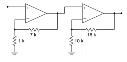
Using only LF411 op amps, design a circuit with an upper break frequency of 500 kHz and a gain of 26 dB.
A gain of 26 dB translates to an ordinary gain of 20. Assuming a noninverting voltage stage, and noting that 𝐴𝑛𝑜𝑖𝑠𝑒=𝐴𝑣 for noninverting form, a single op amp would require an 𝑓𝑢𝑛𝑖𝑡𝑦 of:
![]()
![]()
Because the 411 has a typical 𝑓𝑢𝑛𝑖𝑡𝑦 of 4 MHz, at least two stages are required.
There are many possibilities. One option is to set one stage as the dominant stage and set its gain to produce the desired 𝑓2 . The second stage will then be used to make up the difference in gain to the desired system gain.
Stage 1:
![]()
![]()
![]()
![]()
Stage 2: To achieve a final gain of 20, stage two requires a gain of 2.5. Its 𝑓2 is:
![]()
![]()
![]()
Note that if this frequency worked out to less than 500 kHz, three or more stages would be needed. To set the resistor values, the rules of thumb presented in Chapter Four may be used. One possible solution is shown in Figure 5.3.7 .
Low Frequency Limitations
As mentioned earlier, standard op amps are direct-coupled. That is, their gain response extends down to 0 Hz. Consequently, many op amp circuits have no lower frequency limit. They will amplify DC signals just as easily as AC signals. Sometimes it is desirable to introduce a low frequency rolloff. Two cases of this are single-supply biasing (Chapter Four) and interference rejection (the removal of undesired signals, such as low frequency rumble). In both cases, the circuit designer produces a low frequency rolloff (lead network) by introducing coupling capacitors. For single-supply circuits, these capacitors are a necessary evil. Without them, stages would quickly overload from the large DC input. Also, signal sources and loads may be very intolerant of the DC bias potential. The result could be gross distortion or component failure. Even if a circuit uses a normal bipolar supply, a lead network may be used to reduce interference signals. For example, a well-chosen coupling capacitor can reduce 60 Hz hum interference while hardly affecting the quality of a voice transmission. Generally, these coupling capacitors can be simplified into the straightforward lead networks discussed back in Chapter One. (Remember, for lead networks, the highest critical frequency is the dominant one.) Also, if multiple networks are dominant, the resulting critical frequency will be higher than the individual break frequency. The relationship is the mirror image of Equation 5.3.8 . The proof for the following Equation is very similar to that of Equation 5.3.8 , and is left as an exercise.
![Rendered by QuickLaTeX.com \[f_{1-system} = \frac{f_1}{\sqrt{2^{\frac{1}{n}} -1}} \]](https://pressbooks.nscc.ca/app/uploads/quicklatex/quicklatex.com-587791a385fffb681ab2d040f9dcf6e3_l3.png)
(5.3.9)
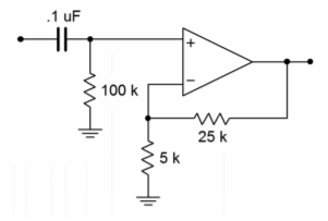
If you decide to add coupling capacitors in order to reduce interference, remember that the op amp will need a DC return resistor. An example is shown in Figure 5.3.8 . The 100 k Ω resistor is needed so that the inverting input’s half of the diff amp stage is properly biased. Note that for a typical op amp, this 100 k Ω also ends up setting the input impedance. Assuming a relatively low source impedance, the lead network simplification boils down to the 0.1 𝜇 F capacitor along with the 100 k Ω . The critical frequency is:
![]()
![]()
![]()
To sum up, then, when using general-purpose op amps, if no signal-coupling capacitors are being used, the gain response extends back to 0 Hz. If coupling capacitors are used, general lead network analysis techniques can be used to find the critical frequencies.

