11.4 Slew Rate and Power Bandwidth
As noted in the previous section, general-purpose op amps contain a compensation capacitor that is used to control the open loop frequency response. The signal developed across this capacitor will be amplified in order to create the final output signal. In essence, this capacitor serves as the load for the preceding stage inside of the op amp. Like all stages, this one has a finite current output capability. Due to this, the compensation capacitor can be charged no faster than a rate determined by the standard capacitor charge equation:
![]()
![]()
The rate of change of voltage versus time is 𝑑𝑣/𝑑𝑡 . By definition, this parameter is called slew rate (SR). The base unit for slew rate is volts per second, however, given the speed of typical devices, slew rate is normally specified in volts per microsecond. Slew rate is very important in that it helps determine whether or not a circuit can accurately amplify high-frequency or pulse-type waveforms. In order to create a fast op amp, either the charging current 𝑖 must be large, or the compensation capacitor 𝐶 must be very small. Because 𝐶 also plays a role in determining the gain bandwidth product, there is a lower limit to its size. A typical op amp might use a 30 pF compensation capacitor, and the driving stage may effectively produce a charging current of 100 𝜇 A. The resulting slew rate would be:
![]()
![]()
![]()
![]()
This means that the output of the op amp can change no faster than 3.33 V over the course of one microsecond. It would take this op amp about 3 microseconds for its output signal to change a total of 10 V. It can go no faster than this. The ideal op amp would have an infinite slew rate. Although this is a practical impossibility, it is possible to find special high-speed devices that exhibit slew rates in the range of several thousand volts per microsecond. Comparative slew rates for a few selected devices are found in Table 11.4.1 .
| Device | Slew Rate |
|---|---|
| uA741 | 0.5 V/ 𝜇 s |
| LF411 | 15 V/ 𝜇 s |
| OPA134 | 20 V/ 𝜇 s |
| LM318 | 70 V/ 𝜇 s |
| LM6364 | 300 V/ 𝜇 s |
| LT1363 | 1000 V/ 𝜇 s |
Table 11.4.1
Slew rate is always output-referred. This way, the circuit gain need not be taken into account. Slew rate is normally the same regardless of whether the signal is positive or negative going. There are a few devices that exhibit an asymmetrical slew rate. One example is the 3900. It has a slew rate of 0.5 V/ 𝜇 s for positive swings, but shows 20 V/ 𝜇 s for negative swings.
The Effect of Slew Rate on Pulse Signals
An ideal pulse waveform will shift from one level to the other instantaneously, as shown in Figure 5.4.1 .
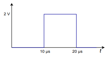
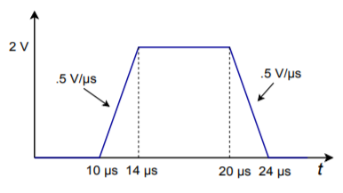
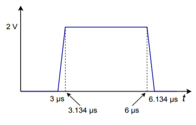
In reality, the rising and falling edges are limited by the slew rate. If this signal is fed into a 741 op amp, the output pulse would be decidedly trapezoidal, as shown in Figure 5.4.2 . The 741 has a slew rate of 0.5 V/ 𝜇 s. Because the voltage change is 2 V, it takes the 741 4 𝜇 s to traverse from low to high, or from high to low. The resulting waveform is still recognizable as a pulse, however.
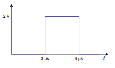
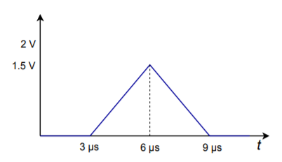
Gross distortion of the pulse occurs if the pulse width is decreased, as in Figure 5.4.3 . Here, the pulse width is only 3 microseconds, so the 741 doesn’t even have enough time to reach the high level. In 3 microseconds, the 741 can only change 1.5 V. By the time the 741 gets to 1.5 V, the input signal is already swinging low, so the 741 attempts to track it. The result is a triangular waveform of reduced amplitude as shown in Figure 5.4.4 . This same effect can occur if the amplitude of the pulse is increased. Obviously, then, pulses that are both fast and large require high slew rate devices. Note that a 411 op amp would produce a nice output in this example. Because its slew rate is 15 V/ 𝜇 s, it requires only 0.134 microseconds for the 2 V output swing. Its output waveform is shown in Figure 5.4.5 .
The Effect of Slew Rate on Sinusoidal Signals and Power Bandwidth
Slew rate limiting produces an obvious effect on pulse signals. Slew rate limiting can also affect sinusoidal signals. All that is required for slewing to take place is that the signal change faster than the device’s slew rate. If the rate of change of the signal is never greater than the slew rate, slewing will never occur. To find out just how fast a given sine wave does change, we need to find the first derivative with respect to time. Assume that the input sine wave has a frequency 𝑓 , and a peak amplitude 𝐾 .
![]()
![]()
The rate of change of the signal with respect to time is 𝑑𝑣/𝑑𝑡 . The maximum rate of change will occur when the sine wave passes through zero (i.e., at t = 0). To find this maximum value, substitute 0 in for t, and solve the equation.
![]()
(5.4.1)
So, the rate of change of the signal is directly proportional to the signal’s frequency ( 𝑓 ), and its amplitude ( 𝐾 ). From this, it is apparent that high-amplitude, high-frequency signals require high slew rate op amps in order to prevent slewing. We can rewrite our Equation in a more convenient form:
![]()
(5.4.2)
where 𝑉𝑝 is the peak voltage swing required and 𝑓𝑚𝑎𝑥 is the highest frequency sine wave reproduced. Often, it is desirable to know just how “fast” a given op amp is. A further rearranging yields
![]()
In this case, 𝑓𝑚𝑎𝑥 represents the highest frequency sine wave that the op amp can reproduce without producing Slewing Induced Distortion (SID). This frequency is commonly referred to as the power bandwidth. To be on the conservative side, set 𝑉𝑝 to the op amp’s clipping level. Note that slew rate calculations are not dependent on either the circuit gain or small-signal bandwidth. Power bandwidth and small signal bandwidth ( 𝑓2 ) are not the same thing. This is a very important point!
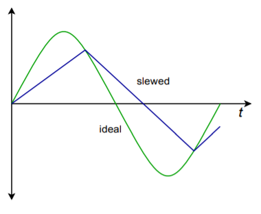
The effects of slewing can be either subtle or dramatic. Small amounts of SID are very difficult to see directly on an oscilloscope and require the use of a distortion analyzer or a spectrum analyzer for verification. Heavy slewing will turn a sine wave into a triangular wave. An example of this is shown in Figure 5.4.6 .
Example 5.4.1
A 741 is used as part of a motor control system. If the highest reproducible frequency is 3 kHz and the maximum output level is 12 V peak, does slewing ever occur?
Another way of stating the problem is to ask “Is the 741’s power bandwidth at least 3 kHz?”
![]()
![]()
![]()
![]()
For this application, the 741 is twice as fast as it needs to be. Note in the calculation how the slew rate is transferred from V/ 𝜇 s into V/s, and how the volts units cancel between denominator and numerator. This leaves units of “1/seconds”, which is another way of saying “Hertz”. If the calculation produced a smaller value, say 2 kHz, then slewing is a possibility for certain signals.
Example 5.4.2
An audio pre-amplifier needs to reproduce signals as high as 20 kHz. The maximum output swing is 10 V peak. What is the minimum acceptable slew rate for the op amp used?
![]()
![]()
![]()
![]()
For this design, a 741 would not be fast enough. The aforementioned 411 through 318 would certainly be satisfactory, whereas the 1363 would probably be overkill.
Computer Simulation
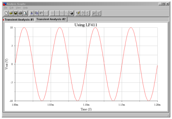
To verify the results of Example 5.4.2 , a simple noninverting voltage amplifier may be used with differing op amp models. The simulation is shown Figure 5.4.7 using Multisim.
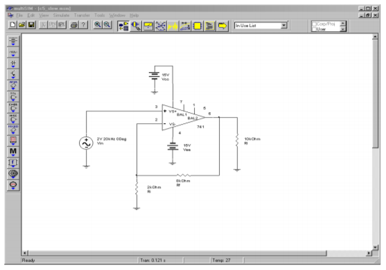
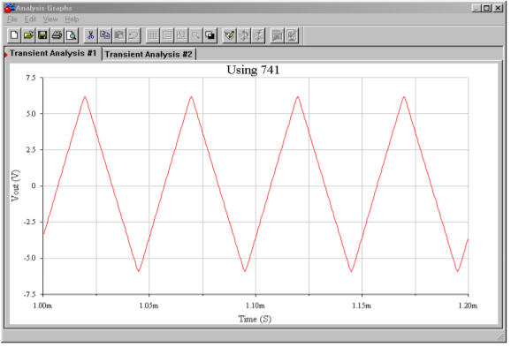
The circuit is configured with a 2 volt input at 20 kHz and a gain of 5. This will yield the worst case output of 10 volts at 20 kHz. For the first Transient Analysis, a 741 is used. Note how the output waveform is essentially triangular. It is also below the expected peak output level. Clearly, this waveform is severely slewed, and results in undesired distortion and a reduction in audio quality.
The second simulation is performed using the faster LF411. In this case, the simulation shows a full 10 volt peak output with no discernable distortion. The LF411 would certainly meet the circuit requirements.
Design Hint
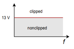
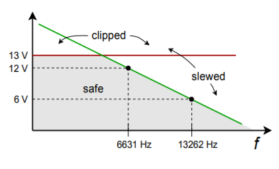
There is a convenient way of graphically determining whether the output of an op amp will be distorted. It involves graphing output levels versus frequency. The two major distortion causes are clipping and slewing. We start with a grid measuring frequency on the horizontal axis, and output voltage on the vertical axis. The first step involves plotting the output level limit imposed by clipping. Clipping is dependent on the circuit’s power supply and is independent of frequency. Therefore, a horizontal line is drawn across the graph at the clipping level (see Figure 5.4.8 ). If we assume a standard ± 15 V power supply, this level will be around ± 13 V. The output level cannot swing above this line because clipping will be the result. Everything below this line represents unclipped signals. The second step is to plot the slewing line. To do this, a point needs to be calculated for 𝑓𝑚𝑎𝑥 . In Example 5.4.1 a 741 was used and 12 V produced an fmax of 6631 Hz. Plot this point on the graph. Now, as the slew rate is directly proportional to 𝑓𝑚𝑎𝑥 and 𝑉𝑝 , it follows that doubling 𝑓𝑚𝑎𝑥 while halving 𝑉𝑝 results in the same slew rate. This new point lets you graphically determine the slope of the slew limiting line. Plot this new point and connect the two points with a straight line (see Figure 5.4.9 ). Everything above this line represents slewed signals, and everything below this line represents non-slewed signals. As long as the desired output signal falls within the lower intersection area of the two lines, the signal will not experience either slewing or clipping. A quick glance at the graph allows you to tell what forms of distortion may affect a given signal.
Slew Rate and Multiple Stages
Consider the three-stage circuit shown in Figure 5.4.10 . The slew rates for each device are found in Table 5.4.1 . What is the effective slew rate of the system? You might think that it is set by the slowest device (741 at 0.5 V/ 𝜇 s), or perhaps by the final device (318 at 70 V/ 𝜇 s). The fact is that the system slew rate could be set by any of the devices, and it depends on the gains of the stages.

The one thing that you can say immediately is that the system slew rate will never be faster than the final device. In this example, the slew rate cannot be greater than 70 V/ 𝜇 s. It may be less than this, however. The trick to finding the effective system slew rate is to start at the output of the first stage, and then determine the maximum rate of change for the following stages in sequence. Looking at stage 1, its maximum output rate is 0.5 V/ 𝜇 s. This is the maximum rate of change going into stage 2. Because stage 2 has a gain of 32, it will attempt to increase this rate to 16 V/ 𝜇 s. This cannot happen, however, because the 411 has a slew rate of only 15 V/ 𝜇 s. Therefore the 411 is the limiting factor at this point. The maximum rate of change out of stage 2 is 15 V/ 𝜇 s. This signal is then applied to stage 3, which has a gain of 3. So, the 318 triples its input signal to 45 V/ 𝜇 s. Because the 318 is capable of changing as fast as 70 V/ 𝜇 s, 45 V/ 𝜇 s becomes the limiting output factor. The system slew rate is 45 V/ 𝜇 s. This is the value used to calculate the system power bandwidth, if needed. The first op amp to slew in this circuit is the 411, even though it is about 30 times faster than the 741 used in stage 1. The reason for this is that it must handle signals 32 times as large. Note that if the final stage had a larger gain, say 5, the 318 would become the limiting factor. The important thing to remember is that the front end stages of a system don’t need to be as fast as the final stages, as they handle smaller signals.
Noncompensated Devices
As discussed in Chapter Three, all op amps need some form of frequency compensation in order to ensure that their closed loop response is stable. The most straightforward way to do this is to add a compensation capacitor, which forces a 20 dB/decade rolloff to 𝑓𝑢𝑛𝑖𝑡𝑦 . In this way, no matter what gain you choose, the circuit will be stable. Although this is very convenient, it is not the most efficient form of compensation for every circuit. High-gain circuits need less compensation capacitance than a low-gain circuit does. The advantage of using a smaller compensation capacitor is that slew rate is increased. Also, available loop gain at higher frequencies is increased. This allows the resulting circuit to have a wider small-signal bandwidth (the effect is as if 𝑓𝑢𝑛𝑖𝑡𝑦 increased). Therefore, if you are designing a high gain circuit, you are not producing the maximum slew rate and small-signal bandwidth that you might. The compensation capacitor is large enough to achieve unity gain stability, but your circuit is a high-gain design. The bottom line is that you are “paying” for unity gain stability with slew rate and bandwidth.
To get around this, manufacturers offer noncompensated op amps. No internal capacitor is used. Instead, connections are brought out to the IC package so that you may add your own capacitor. This way, the op amp may be tailored to your application. There is no set way of determining the values for the external compensation circuit (it may be more complex than a single capacitor). Compensation details are given on manufacturers data sheets. One example of a noncompensated op amp is the 301. You can think of a 301 as a 741 without a compensation capacitor. If a 33 pF compensation capacitor is used, the 301 will be unity gain stable and produce an 𝑓𝑢𝑛𝑖𝑡𝑦 of 1 MHz and a slew rate of 0.5 V/ 𝜇 s. For higher gains, a smaller capacitor may be used. A 10 pF unit will produce an effective 𝑓𝑢𝑛𝑖𝑡𝑦 of 3 MHz, and a slew rate of 1.5 V/ 𝜇 s. Comparative Bode gain plots are shown in Figure 5.4.11 for the 301.

Feedforward Compensation
Besides the ordinary form of compensation, noncompensated devices like the 301 may utilize other methods that can make them even faster, such as feedforward compensation. The concept of feedforward is in direct contrast to feedback. As its name suggests, feedforward involves adding a portion of the input signal to the output, thus bypassing certain sections of the system. Compared to ordinary feedback, feedforward is seldom used as part of the design of an amplifier.[1]
Ordinarily, a compensation capacitor must be large enough to maintain sufficient gain and phase margin for the slowest stage inside of an op amp. Quite often, the slowest stage in an op amp is one of the first stages, such as a level shifter. Here is where feedforward comes into play. If the high frequency content of the input signal can be shunted around this slow stage, the effective bandwidth and speed of the op amp may be increased. This is the key behind the technique of feedforward compensation. Normally, manufacturers will provide details of specific feedforward realizations for their op amps. (It would be very difficult to create successful feedforward designs without detailed knowledge of the internal design of the specific op amp being used.) Not all op amps lend themselves to feedforward techniques.
In summary, noncompensated op amps require a bit more work to configure than fully compensated devices, but offer higher performance. This means faster slew rates and higher-upper break frequencies.
Decompensated Devices
Straddling the worlds of compensated and uncompensated op amps is the decompensated device. Decompensated devices are also known as partially compensated devices. They include some compensation capacitance, but not enough to make them unity gain stable. Usually these devices are stable for gains above 3 to 5. Because the majority of applications require gains in this area or above, decompensated devices offer the ease of use of compensated devices and the increased performance of customized noncompensated units. If required, extra capacitance can usually be added to make the circuit unity gain stable. One example of this type is the 5534. Its gain Bode plot is shown in Figure 5.4.12 . Note how the addition of an extra 22 pF reduces the open loop gain. This 22 pF is enough to make the device unity gain stable. It also has a dramatic effect on the slew rate, as seen in the 5534’s spec sheet. Without the 22 pF capacitor, the slew rate is 13 V/ 𝜇 s, but with it, the slew rate drops to 6 V/ 𝜇 s. The performance that you give up in order to achieve unity gain stability is obvious here.
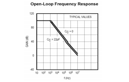
There is one more interesting item to note about the 5534. A close look at the Bode gain curve shows a hump in the rolloff region. Some other devices, such as the 318, exhibit this hump too. This is a nice extra. In essence, the manufacturer has been able to achieve a slightly higher open loop gain than a normal device would allow. This means that your circuits will have higher loop gains, and therefore, the nice effects of negative feedback will remain active to higher frequencies. This also means that very high gain circuits will be able to achieve a higher 𝑓2 than is predicted by the gain-bandwidth calculation.
- It can offer similar advantages though, such as a reduction in distortion. Also, feedforward and feedback techniques may be combined in order to achieve complementary increases in performance. For an example, see M.J.Hawksford, “Reduction of Transistor Slope Impedance Dependent Distortion in Large Signal Amplifiers”,Journal of the Audio Engineering Society, Vol.36 No.4 (1988): 213–222 ↵

