8.2 What Is An Op Amp?
An operational amplifier is, in essence, a multi-stage high gain amplifier treated as a single entity. Normally, op amps have a differential input and a single-ended output. In other words, one input produces an inverted output signal, and the other input produces a noninverted output signal. Often, the op amp is driven from a bipolar power supply (i.e., two supplies, one positive and one negative). Just about any sort of active amplifying device may be used for the individual stages. Op amps can be made entirely from vacuum tubes or discrete bipolar transistors (and of course, they were made that way some years ago). The advances in semiconductor manufacture in the late 1960’s and early 1970’s eventually made it possible to miniaturize the required components and place the whole affair on a single silicon chip (hence the term, integrated circuit). Through common use, this is what is generally meant by the term op amp today.
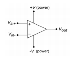
As seen in Figure 8.2.1 , a typical op amp has at least five distinct connections; an inverting input (labeled “-”), a noninverting input (labeled “+”), an output, and positive and negative power supply inputs. These power supply connections are sometimes referred to as supply rails. Note that a ground connection is not directly given. Rather, a ground connection is implied through the other connections. This symbol and its associated connections are typical, but by no means absolute. There are a wide variety of devices available to the designer that offer such features as differential outputs or unipolar power supply operation. In any case, some form of triangle will be used for the schematic symbol.
It is best to think of op amps as general-purpose building blocks. With them, you can create a wide variety of useful circuits. For general-purpose work, designing with op amps is usually much quicker and more economical than an all-discrete approach. Likewise, trouble shooting and packaging constraints may be lessened. For more demanding applications, such as those requiring very low noise, high output current and/or voltage, or wide bandwidth, manufacturers have created specialized op amps. The final word in performance today is still dominated by discrete circuit designs though. Also, it is very common to see a mix of discrete and integrated devices in a given circuit. There is certainly no law that states that op amps can only be used with other op amps. Often, a judicious mix of discrete devices and op amps can produce a circuit superior to one made entirely of discretes or op amps alone.
Where might you find op amp circuits? In a word, anywhere. They’re probably in use in your home stereo or TV where they help capture incoming signals, in electronic musical instruments where they can be used to create and modify tones, in a camera in conjunction with a light metering system, or in medical instruments where they might be used along with various bio-sensing devices. The possibilities are almost endless.
Block Diagram Of An Op Amp
At this point you may be asking yourself, “what’s inside of the op amp?” The generic op amp consists of three main functional stages. A real op amp may contain more than three distinct stages, but can be reduced to this level for analysis. A generalized discrete representation is given in Figure 8.2.2 . Since the op amp requires a differential input scheme, the first stage is most often a differential amplifier. As seen here, 𝑄1 and 𝑄2 comprise a PNP-based differential amplifier. The output of one collector ( 𝑄2 here) is then fed to a high-gain second stage. This stage usually includes a lag network capacitor that plays a major roll in setting the op amp’s AC characteristics (this is examined further in Chapter Five). 𝑄3 makes up the second stage in the example. It is set in a common emitter configuration for both current and voltage gain. The a-fore mentioned lag capacitor is positioned across 𝑄3 ‘s base-collector junction in order to take advantage of the Miller effect. The third and final section is a class B or class AB follower for the most effective load drive. 𝑄4 and 𝑄5 make up the final stage. The twin diodes compensate for the 𝑄4 and 𝑄5 𝑉𝐵𝐸 drops, and produce a trickle bias current that minimizes distortion. This is a relatively standard class AB stage. Note that the entire circuit is direct-coupled. There are no lead networks, and thus the op amp can amplify down to zero Hertz (DC). There are many possible changes that may be seen in a real world circuit, including the use of Darlington pairs or FETs for the differential amplifier, multiple high gain stages, and output current limiting for the class B section.
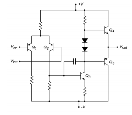
The example discrete circuit uses only five transistors and two diodes. In contrast, an integrated version may use two to three dozen active devices. Because of the excellent device matching abilities of single chip integration, certain techniques are used in favor of standard discrete designs. Internal IC current sources are normally made through the use of current mirrors. Current mirror configurations are also employed to create active loads, in order to achieve maximum circuit gain.
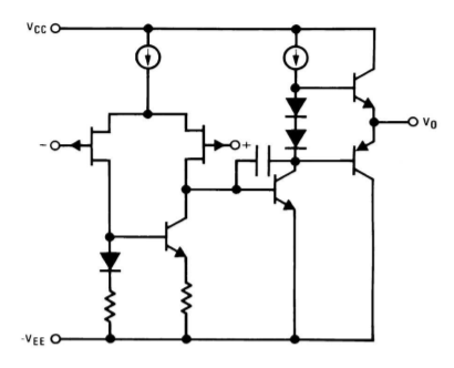
A typical integrated op amp will contain very few resistors, and usually only one or two lag network capacitors. Due to size limitations and other factors, inductors are virtually unseen in these circuits. A simplified equivalent circuit of the LF411 op amp is shown in Figure 8.2.3 . Note that this device uses JFETs for the diff amp with an active load. The diff amp tail current source and the class AB trickle bias source are shown as simple current sources. In reality, they are a bit more complex, utilizing current mirror arrangements.
One of the most popular op amps over the years has been the 741. The specifications of this device seem rather lackluster by today’s standards, but it was one of the first easy-to-use devices produced. As a result, it has found its way into a large number of designs. Indeed, it is still a wise choice for less demanding applications, or where parts costs are a major consideration. A complete schematic of the 𝜇 A 741 is shown in Figure 8.2.4 . Several different manufacturers make the 741. This version is manufactured by Signetics, and may be somewhat different than a 741 made by another company.[1] The circuit contains 20 active devices and about one dozen resistors.
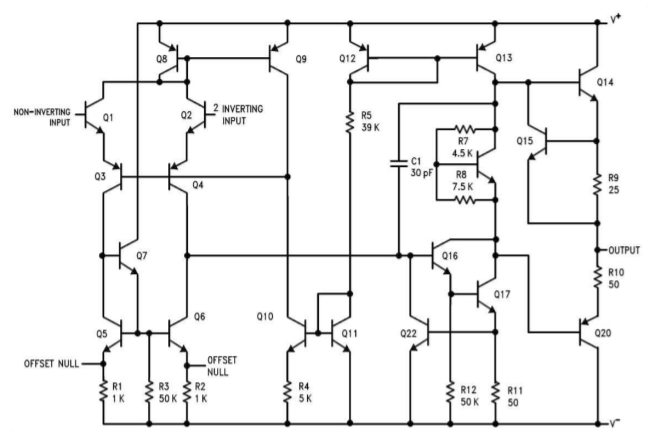
At first glance, this circuit may look hopelessly confusing. A closer look reveals many familiar circuit blocks. First off, you will notice that a number of devices show a shorting connection between their base and collector terminals, such as 𝑄8 , 𝑄11 , and 𝑄12 . In essence, these are diodes (they are drawn this way because they are manufactured as transistor junctions. It is actually easier to make diodes in this fashion). For the most part, these diodes are part of current mirror biasing networks. The bias setup is found in the very center of the schematic, and revolves around 𝑄9 through 𝑄12 . The setup current is found by subtracting two diode drops ( 𝑄11,\(𝑄12 ) from the total power supply potential ( 𝑉+−𝑉− ), and dividing the result by 𝑅5 . For a standard ±15 V power supply, this works out to
![]()
![]()
![]()
This current is reflected into 𝑄13 . A close look at 𝑄10 and 𝑄11 reveals that this portion is not a simple current mirror. By including 𝑅4 , the voltage drop across the base emitter of 𝑄10 is decreased, thus producing a current less than 733𝜇𝐴 . This configuration is known as a Widlar current source. The derivation of the exact current Equation is rather involved, and beyond the scope of this chapter.[2] This current is reflected into 𝑄8 via 𝑄9 , and establishes the tail current for the differential amplifier. The diff amp stage uses a total of four amplifying transistors in a common-collector/common-base configuration (𝑄1 through 𝑄4). In essence, 𝑄1 and 𝑄2 are configured as emitter followers, thus producing high input impedance and reasonable current gain. 𝑄3 and 𝑄4 are configured as common base amplifiers, and as such, produce a large voltage gain. The gain is maximized by the active load comprised of 𝑄5 through 𝑄7. The output signal at the collector of 𝑄4 passes on to a dual transistor high-gain stage ( 𝑄16 and 𝑄17). 𝑄16 is configured as an emitter follower and buffers 𝑄17 , which is set as a common emitter voltage amplifier. Resistor 𝑅11 serves to stabilize both the bias and gain of this stage (i.e., it is an emitter degeneration or swamping resistor). 𝑄17 is directly coupled to the class AB output stage ( 𝑄14 and 𝑄20 ). Note the use of a𝑉𝐵𝐸 multiplier to bias the output transistors. The 𝑉𝐵𝐸multiplier is formed from 𝑄18 and resistors 𝑅7 and 𝑅8 . Note that this section receives its bias current from 𝑄13 which is part of the central current mirror complex.
Some transistors in this circuit are used solely for protection from overloads. A good example of this is 𝑄15. As the output current increases, the voltage across 𝑅9 will increase proportionally. Note that this resistor is in parallel with the base emitter junction of 𝑄15 . If this potential gets high enough, 𝑄15 will turn on, shunting base drive current around the output device (𝑄14). In this manner, current gain is reduced, and the maximum output current is limited to a safe value. This limiting value may be found via Ohm’s Law:
![]()
![]()
![]()
In a similar fashion, 𝑄20 is protected by 𝑅10 , 𝑅11 , and 𝑄22 . If the output tries to sink too large of a current, 𝑄22 will turn on, shunting current away from the base of 𝑄16 . While individual op amp schematics will vary widely, they generally hold to the basic four-part theme presented here:
- A central current source/current mirror section to establish proper bias.
- A differential amplifier input stage with active load.
- A high voltage gain intermediate stage.
- A class B or AB follower output section.
Fortunately for the designer or repair technician, intimate knowledge of a particular op amp’s internal structure is usually not required for successful application of the device. In fact, a few simple models can be used for the majority of cases. One very useful model is given in Figure 8.2.5 .
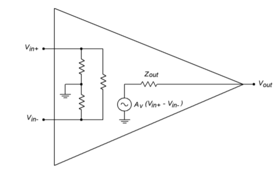
Here the entire multistage op amp is modeled with a simple resistive input network, and a voltage source output. This output source is a dependent source. Specifically, it is a voltage-controlled voltage source. The value of this source is
![]()
The input network is specified as a resistance from each input to ground, as well as an input-to-input isolation resistance. For typical op amps these values are normally hundreds of kilo-ohms or more at low frequencies. Due to the differential input stage, the difference between the two inputs is multiplied by the system gain. This signal is presented to the output terminal through the final stage’s output impedance. The output impedance will most likely be less than 100 Ω . System voltage gains in excess of 80 dB (10,000) are the norm.
A Simple Op Amp Simulation Model
It is possible to create a great variety of simulation models for any given op amp. Generally speaking, the more accurate the model is, the more likely it is to be complex. Due to the nature of most simulators, a more complex model requires a greater amount of time for an analysis to be completed. There is always a trade-off between model complexity and computation time. We can create a very simple model based on the previous section. This model is shown in Figure 8.2.6 .
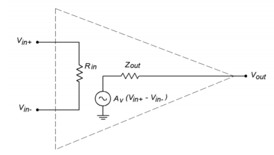
It consists of just five nodes. The input section is modeled as a single resistor, 𝑅𝑖𝑛 , between nodes 1 and 8. These two nodes are the noninverting and inverting inputs of the op amp, respectively. The second half of the model consists of a voltage controlled voltage source and an output resistor. The value of this dependent source is a function of the differential input voltage and the voltage gain. With a minimum of components, the simulation time for this model is very low. In order to use this model, you need only set three parameters, the input resistance, the output resistance, and the voltage gain. An example is shown in Figure 8.2.7 using Multisim.
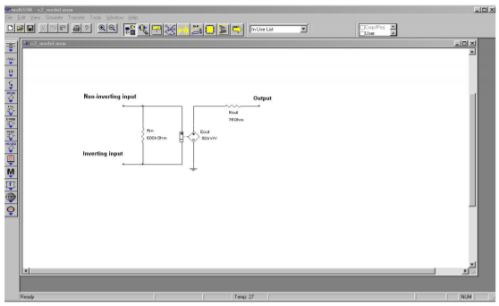
This model must be used with great care because it is so simplistic. It is useful as a learning tool for investigating the general operation of an op amp, but should never be considered as part of a true-to-life simulation. This model makes no attempt to consider the many limitations of the op amp. Because this model in no way imposes output signal swing limits, the effects of saturation will go unnoticed. Similarly, no attempt has been made at modeling the frequency response of the op amp. This is of great concern and we will spend considerable time on this subject in later chapters. Many other effects are also ignored. With so many limitations, you might wonder just where such a model may be used. This model is useful for non-critical simulations given low frequency inputs. You must also recognize the onset of saturation (clipping) yourself. Its primary advantage is that the circuit model is small, and thus computationally fast. Because of this, it is very efficient for students who are new to both op amps and circuit simulation. Perhaps of equal importance, is the fact that this model points out the fact that your simulation results can only be as good as the models you use. Many people fall into the trap that “because the simulation came from a computer, it must be correct”. Nothing could be further from the truth. Always remember the old axiom: GIGO (Garbage In = Garbage Out). It can be very instructive to simulate a circuit using differing levels of accuracy and complexity, and then noting how closely the results match the same circuit built in the laboratory.
Op Amp Data Sheet and Interpretation
Different manufacturers often use special codes and naming conventions to delineate their products from those of other manufacturers, as well as providing quality level and manufacturing information. A manufacturer’s code is usually a letter prefix, while a quality or construction code is a suffix. Common prefix codes include 𝜇 A (Fairchild), AD (Analog Devices), CS (Crystal), LM, LH, and LF (National Semiconductor, now owned by Texas Instruments, with M indicating monolithic construction, H indicating hybrid construction, and F indicating an FET device), LT (Linear Technology), MC (Motorola), NE and SE (Signetics), OPA (Burr-Brown), and TL (Texas Instruments).
Many manufacturers make a host of standard parts such as the 741. For example, Texas Instruments makes the LM741, while Fairchild makes the 𝜇 A741. These parts are generally considered to be interchangeable, although they may vary in some ways. Some manufacturers will use the prefix code of the original developer of a part, and reserve their prefix for their own designs. As an example, Signetics produces their version of the 741, that they call 𝜇 A741 because this op amp was first developed by Fairchild. (Signetics is then referred to as a second source for the 𝜇 A741).
Suffix codes vary widely between manufacturers. Typical designations for consumer grade parts are C, and CN. The suffix N often means Not Graded. Interestingly, the lack of a final suffix often indicates a very high quality part, usually with an extended temperature range. Suffix codes are also used to indicate package styles. This practice is particularly popular among voltage regulators and other high-power linear ICs.
Finally, some manufacturers will use a “parallel” numbering system for high-grade parts. For example, the commercial grade device may have a “300 series” part number, with industrial grade given a “200 series” designation, and a military grade part given a “100 series” number. One possible example is the LM318 commercial grade op amp versus its high-grade counterpart, the LM118. Generally, militaryspecified parts will have a very wide temperature range, with industrial and commercial grades offering progressively less.
The data sheet for the LF411 op amp is shown in Figure 8.2.8 . Let’s take a look at some of the basic parameters and descriptions. The values given are typical of a modern op amp. A complete investigation of all parameters will be given in Chapter Five, once we’ve gotten a little more familiar with the device.


First, note that two versions of the IC are given. We will examine the LF411 rather than the high-grade LF411A. At the very top of the data sheet is a listing of the absolute maximum ratings. The op amp should never operate at values greater than those presented as doing so may permanently damage it. Like most general-purpose op amps, the LF411 is powered by a bipolar power supply. The supply rails should never exceed ± 18 V DC. Normally, op amps will be used with ± 15 V supplies. Maximum power dissipation is given as 670 mW. Obviously then, this is a small signal device. In keeping with this, the operating temperature range and maximum junction temperatures are relatively low. We also see that the device can withstand differential input signals of up to 30 V, and single-ended inputs of up to 15 V, without damage. On the output, the LF411 is capable of withstanding a shorted load condition continuously. This makes the op amp a bit more “bullet-proof”. The remainder of this section details soldering conditions. Excessive heat during soldering may damage the device.
The second section of the data sheet lists the DC characteristics of the op amp. This table is broken down into five major sections:
- The parameter symbol.
- The parameter name.
- The conditions under which the parameter is measured.
- The parameter values, either typical or min/max.
- The parameter units.
We will examine a few of these parameters right now. The fourth parameter given is 𝐼𝐵 , the input bias current. 𝐼𝐵 is the current drawn by the bases (or gates) of the input differential amplifier stage. Because the LF411 utilizes a JFET diff amp, we expect this value to be rather small. For an operating temperature of 25°C, a typical LF411 will draw 50 pA, and a worst-case LF411 no more than 200 pA. If we extend the temperature range out a bit, 𝐼𝐵 can extend out to 50 nA. This is a sizable jump, but even 50 nA is a very small value for general-purpose work. Because larger bias currents are normally seen as undesirable, the maximum 𝐼𝐵 is the worst case scenario, hence a minimum 𝐼𝐵 is not reported. Along with this, we see a very high value for input resistance, some 1012Ω , typically. Op amps utilizing bipolar input devices will show much higher values for 𝐼𝐵 , and much lower values for 𝑅𝑖𝑛 .
Next in line comes 𝐴𝑣𝑜𝑙 . This is the DC voltage gain. Note the test conditions. The power supply is set to ± 15 V, the load is 2 k Ω , and 𝑉𝑜𝑢𝑡 is 10 V peak. Normally, we desire as much gain as possible, so the worst case scenario is the minimum 𝐴𝑣𝑜𝑙 . For 25∘ C operation this is specified as 25 V/mV, or 25,000. The average device will produce a gain of 200,000. As is typical, once the temperature range is expanded performance degrades. Over the operating temperature range, the minimum gain may drop to 15,000.
Because the op amp uses a class AB follower for its output stage, we should expect the output compliance to be very close to the power supply rails. The output voltage swing is specified for ± 15 V supplies with a 10 k Ω load. The typical device can swing out to ± 13.5 V, with a worst case swing of ± 12 V. A reduction in power supply value will naturally cause the maximum output swing to drop. A sizable reduction in the load resistance will also cause a drop in 𝑉𝑜 , as we will see a bit later. These maximum output values are caused by the internal stages reaching their saturation limits. When this happens, the op amp is said to be clipping or in saturation. As a general rule of thumb, saturation may be approximated as 1.5 V less than the magnitude of the power supplies.
The last item in the list is the standby current draw, 𝐼𝑆 . Note how small this is, only 1.8 mA, 3.4 mA worst case. This is the current the op amp draws from the supply under no signal conditions. When producing output signals, the current draw will rise.
The final section of the data sheet lists certain AC characteristics of the op amp that will be of great concern to us in later sections. Many device parameters change a great deal with frequency, temperature, supply voltage, or other factors. Because of this, data sheets also include a large number of graphs that further detail the op amp’s performance. Finally, application hints and typical circuits may round out the basic data sheet.
- While the exact internal circuitry may be altered, the various manufacturers versions will have the same pinouts, and very similar performance specifications. ↵
- A complete derivation of the Widlar current source may be found in Principles of Electronic Circuits, by S.G.Burns and P.R.Bond, 1987, West Publishing Company. ↵

