8.3 Simple Op Amp Comparator
Now that you have a feel for what an op amp is and what some typical parameters are, let’s take a look at an application. The one thing that jumps to most people’s attention is the very high gain of the average op amp. The typical LF411 showed 𝐴𝑣𝑜𝑙 at approximately 200,000. With gains this high, it is obvious that even very small input signals can force the output into saturation (clipping). Take a look at Figure 8.3.1 . Here an op amp is being supplied by ± 15 V, and is driving a 10 k Ω load. As seen in our model of Figure 8.2.5, 𝑉𝑜𝑢𝑡should equal the differential input voltage times the op amp’s gain, 𝐴𝑣𝑜𝑙 .
![]()
![]()
![]()
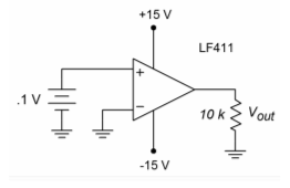
The op amp cannot produce 20,000 V. The data sheet lists a maximum output swing of only ± 13.5 V when using ± 15 V supplies. The output will be truncated at 13.5 V. If the input signal is reduced to only 1 mV, the output will still be clipped at 13.5 V. This holds true even if we apply a signal to the inverting input, as in Figure 8.3.2 .
![]()
![]()
![]()
![]()

Computer Simulation
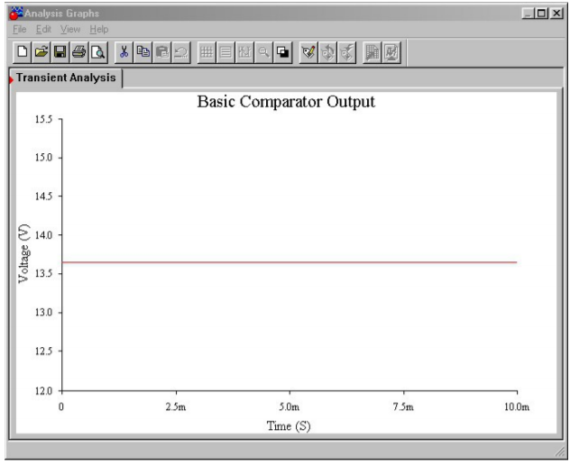
A simulation of Figure 8.3.2 using Multisim is shown in Figure 8.3.3 . The LF411 op amp is selected from the component library, and you need not concern yourself with the model’s internal make-up just yet. This particular model includes the effects of power supply limitations (i.e., output saturation) that the very simple dependent-source model presented earlier does not. Individual DC sources are used for the input signals. Although no AC signals are applied, it is perfectly valid to run a transient-mode simulation. The first millisecond of the output voltage is shown. It verifies the manual calculation, indicating a DC level of slightly more than 13.5 V.
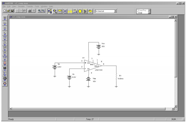
For any reasonable set of inputs, as long as the noninverting signal is greater than the inverting signal, the output will be positive saturation. If you trade the input signals so that the inverting signal is the larger, the converse will be true. As long as the inverting signal is greater than the noninverting signal, the output will be negative saturation. If the inverting and noninverting signals are identical, 𝑉𝑜𝑢𝑡 should be 0 V. In the real world, this will not happen. Due to minute discrepancies and offsets in the diff amp stage, either positive or negative saturation will result. You have no quick way of knowing in which direction it will go. It is for this reason that it is impractical to amplify a very small signal, say around 10 𝜇 V. You might then wonder, “What is the use of this amplifier if it always clips? How can I get it to amplify a simple signal?” Well, for normal amplification uses, we will have to add on some extra components, and through the use of negative feedback (next chapter), we will create some very well-controlled, useful amplifiers. This is not to say that our barren op amp circuit is useless. Quite to the contrary, we have just created a comparator.
A comparator has two output states: High and low. In other words, it is a digital, logical output. Our comparator has a high state potential of 13.5 V, and a low state potential of -13.5 V. The input signals, in contrast, are continuously variable analog potentials. A comparator, then, is an interface between analog and digital circuitry. One input will be considered the reference, while the other input will be considered the sensing line. Note that the differential input signal is the difference between the sensing input and the reference input. When the polarity of the differential input signal changes, the logical output of the comparator changes state.
Example 8.3.1
Figure 2.3.4 shows a light leakage detector that might be used in a photographer’s dark room. This circuit utilizes a Cadmium Sulfide (CdS) cell that is used as a light sensitive resistor. The inverting input of the op amp is being used as the reference input, with a 1 V DC level. The noninverting input is being used as the sensing input. Under normal (no light) conditions, the CdS cell acts as a very high resistance, perhaps 1 M Ω . Under these conditions, a voltage divider is set up with the 10 k Ω resistor, producing about 150 mV at the noninverting input. Remember, no loading of the divider occurs because the LF411 utilizes a JFET input. Because the noninverting input is less than the inverting input, the comparator’s output is negative saturation, or approximately -13.5 V. If the ambient light level rises, the resistance of the CdS cell drops, thus raising the signal applied to the noninverting input. Eventually, if the light level is high enough, the noninverting input signal will exceed the 1 V reference, and the comparator’s output will move to positive saturation, about +13.5 V. This signal could then be used to trigger some form of audible alarm. A real world circuit would need the flexibility of an adjustable reference in place of the fixed 1 V reference. By swapping the CdS cell and the 10 k Ω resistor, and adjusting the reference, an inverse circuit (i.e., an alarm that senses darkness) may be produced.
Circuits of this type can be used to sense a variety of over level/under level conditions, including temperature and pressure. All that is needed is an appropriate sensing device. Comparators can also be used with AC input signals.

Example 8.3.2
Sometimes, it is necessary to square up an AC signal for further processing. That is, we must turn it into an equivalent pulse waveform. One example of this might be a frequency counter. A frequency counter works by tallying the number of high-to-low or low-to-high transitions in the input signal over a specific length of time. For accurate counts, good edge transitions are required. Because a simple sine wave changes relatively slowly compared to an equal frequency square wave, some inaccuracy may creep into the readings. We can turn the input into a pulse-type output by running it through the comparator of Figure 2.3.5 . Note that the reference signal is adjustable from −15 to +15 V. Normally, the reference is set for 0 V. Whenever the input is greater than the reference, the output will be positive saturation. When the input is less than the reference, the output will be negative saturation. By making the reference adjustable, we have control over the output duty cycle, and can also compensate for DC offsets on the input signal. A typical input/output signal set is given in Figure 2.3.6 .
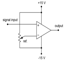
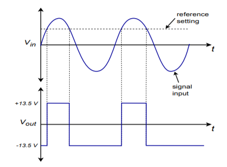
There are a few limitations with our simple op amp comparator. For very fast signal changes, a typical op amp will not be able to accurately track its output. Also, the output signal range is rather wide and is bipolar. It is not at all compatible with normal TTL logic circuits. Extra limiting circuitry is required for proper interfacing. To help reduce these problems, a number of circuits have been specially optimized for comparator purposes. We will take a closer look at a few of them in Chapter Seven.

