8.4 Op Amp Manufacture
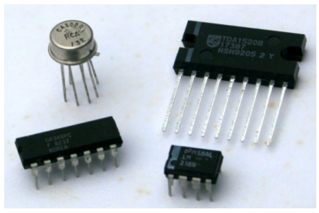
Op amps and other linear integrated circuits are generally manufactured in one of two ways: The device is either a hybrid, or is monolithic. In either case, the circuit can contain hundreds of components. The resulting device will be packaged in a variety of styles, including plastic and ceramic dual in-line and single in-line types, multi-lead cans, flat packs, and surface mount forms. Some examples are shown in Figure 2.4.1 . In each type, the circuitry is completely encased and not accessible to the designer or technician. If one of the components should fail, the entire op amp is replaced. The design and layout of the integrated circuit itself is normally carried out with the use of special computer workstations and software tools. These allow the designers to simulate portions of the circuit, and create the outlines and interconnections for the various components to be formed.

Monolithic Construction
The term monolithic is from the Greek, meaning literally “single stone”. In this process, all circuit elements are created and interconnected using a single slab of silicon (or other suitable material). Normally, several op amps are made from a single silicon wafer. Each wafer may be a few inches in diameter, with each op amp circuit chip comprising perhaps a square 1 millimeter by 1 millimeter in area. A single transistor can easily be smaller than 15 micrometers by 20 micrometers. Because the scale of construction is so small, special clean rooms are required in order to remove tiny air-borne particles of dust and grit that could interfere with the production of these super-small components. Workers in clean rooms are required to wear special suits as well.
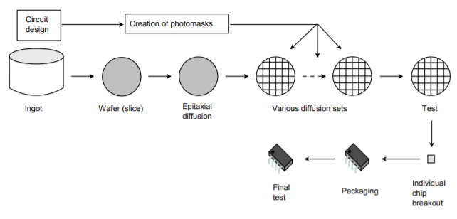
Figure 2.4.2 outlines the major steps in the chip manufacturing process. This process starts with the preparation of a P-type silicon wafer. This is referred to as the substrate. After it has been cleaned and polished, an N-type epitaxial region is diffused into the P-type base. Epitaxial is from the Greek, roughly meaning “to arrange upon”. It is within this thin epitaxial region that the circuit elements will be formed, the remainder of the substrate lending mechanical support to the structure. The term diffusion refers to the manner in which the semiconductor material becomes doped. In essence, the base material is surrounded by a high concentration of doping material, usually gaseous, along with the application of heat. The low concentration wafer material will be infiltrated by the high concentration doping material. Diffusion is a relatively accurate and inexpensive means of controlling the semiconductor’s properties.

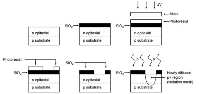
Once the N-type region is produced, the wafer will undergo an oxidizing process that will leave the top surface covered with silicon dioxide. This layer prevents impurities from entering the N-type region. At this point, a series of steps will be used to create wells or deposits of alternate p and n material. These deposits will form the various active and passive components. Normally, this is done through a photolithographic process. This involves the use of light sensitive materials and masks. Conceptually, the process is not very much different from the way printed circuit boards are often made. In essence, specific areas of the silicon dioxide layer will be stripped away, thus exposing the epitaxial region, and allowing diffusion of other acceptor/donor impurities to take place. Because the silicon dioxide serves as an effective barrier to diffusion, only areas cleared of silicon dioxide will be effected by the diffusion process. In this manner, specific areas can be singled out, and selectively doped to create specific components. This is detailed below and in Figure 2.4.3 .
In order to selectively remove the silicon dioxide, the top surface is coated with a light sensitive material called photoresist. Above this is placed a mask. This mask is much like a black and white negative; some areas are clear, and some areas are opaque. The resulting sandwich is then exposed to ultraviolet light. The clear areas of the mask will allow the light to pass through and cause a chemical change in the photoresist. A solution is then used to wash away the unexposed photoresist. At this point, a second solution is used to wash away the silicon dioxide. This solution will not effect the exposed photoresist, and thus, the silicon dioxide beneath it is unaffected. After this protecting layer of photoresist is removed, all that remains on the top surface of the wafer are alternating patches of silicon dioxide. The wafer can now be lead through another diffusion process.

The process of oxidizing, masking, and diffusing will be repeated several times. The initial run will be produced with an isolation mask. This is used to separate the various components. Normally, a base mask will be used next, followed by the emitter mask. The final masks will be used for contacts and interconnections. In this way, N-type material can be placed next to, or completely within, P-type material. The adjoining areas are, of course, PN junctions. Because all circuit elements are laid out length-wise on a thin strip, this form of manufacture is referred to as a planar process.
Once the final mask is completed, the wafer will be inspected. The individual chips will then be broken out of the wafer and mounted into the desired package. Leads will be connected to the chip with fine angel hair wire, and then the package will be sealed. It is now ready for final test and inspection. Part numbers and date codes will also be imprinted.
Virtually all general-purpose op amps today use a planar monolithic process. Some of the advantages of monolithic construction are its relative simplicity and low per-part cost.
Hybrid Construction
Hybrids are usually used where a complete monolithic solution is impractical. This is usually the case for special purpose devices, such as those requiring very high output current, very wide bandwidth, or that are very complex or sensitive. Hybrids, as the name suggests, are a collection of smaller circuit elements interconnected. A typical hybrid may contain two or three smaller monolithic chips and assorted miniaturized passive and/or power components. Passive components may be further integrated by using either a thin or thick film chip process. (A discussion of thin and thick film chip techniques is beyond the scope of this text). Due to the complexity of a hybrid chip, it is normally more expensive than its monolithic cousins. Although the IC itself may be more expensive, the complete application may very well wind up being less costly to produce because the cost of other components are effectively absorbed within the hybrid IC. One place where hybrids are often used is in consumer stereo music systems. A hybrid power amplifier IC offers the convenience of a single IC solution with the capabilities of a discrete transistor approach. As an op amp user, it makes little difference whether the device is hybrid or monolithic when it comes to circuit analysis or design.

